Nano Vacuum Triode Structure and Preparation Method of Inverted Anode

A vacuum triode, anode technology, applied in cold cathode manufacturing, electrode system manufacturing, non-electron emission anode and other directions, can solve the problem of difficult to overcome cathodic oxidation, insufficient collection capacity of device leakage anode, affecting the development and application of aluminum nitride vacuum triode, Insufficient anode collection capacity and other problems, to achieve the effect of reducing manufacturing difficulty, reducing oxidation, and reducing process treatment

Active Publication Date: 2018-06-22
INST OF SEMICONDUCTORS - CHINESE ACAD OF SCI
View PDF4 Cites 0 Cited by
  • Summary
  • Abstract
  • Description
  • Claims
  • Application Information

AI Technical Summary

Problems solved by technology

However, there are certain problems in the manufacturing process of nanometer vacuum triodes at present.
First of all, during the process of growing a multilayer structure on the surface of the cathode, the cathode is in a high temperature and oxygen environment, which easily causes the oxidation of the cathode surface.
Secondly, the anode made by the traditional process is an open structure without lateral confinement, which increases the leakage of the device and leads to insufficient collection capacity of the anode
In summary, the current vacuum triode structure is difficult to overcome the problems of cathode oxidation, device leakage and insufficient anode collection capacity, which affects the development and application of aluminum nitride vacuum triodes.

Method used


Image

  • Nano Vacuum Triode Structure and Preparation Method of Inverted Anode
  • Nano Vacuum Triode Structure and Preparation Method of Inverted Anode

Examples


Embodiment Construction

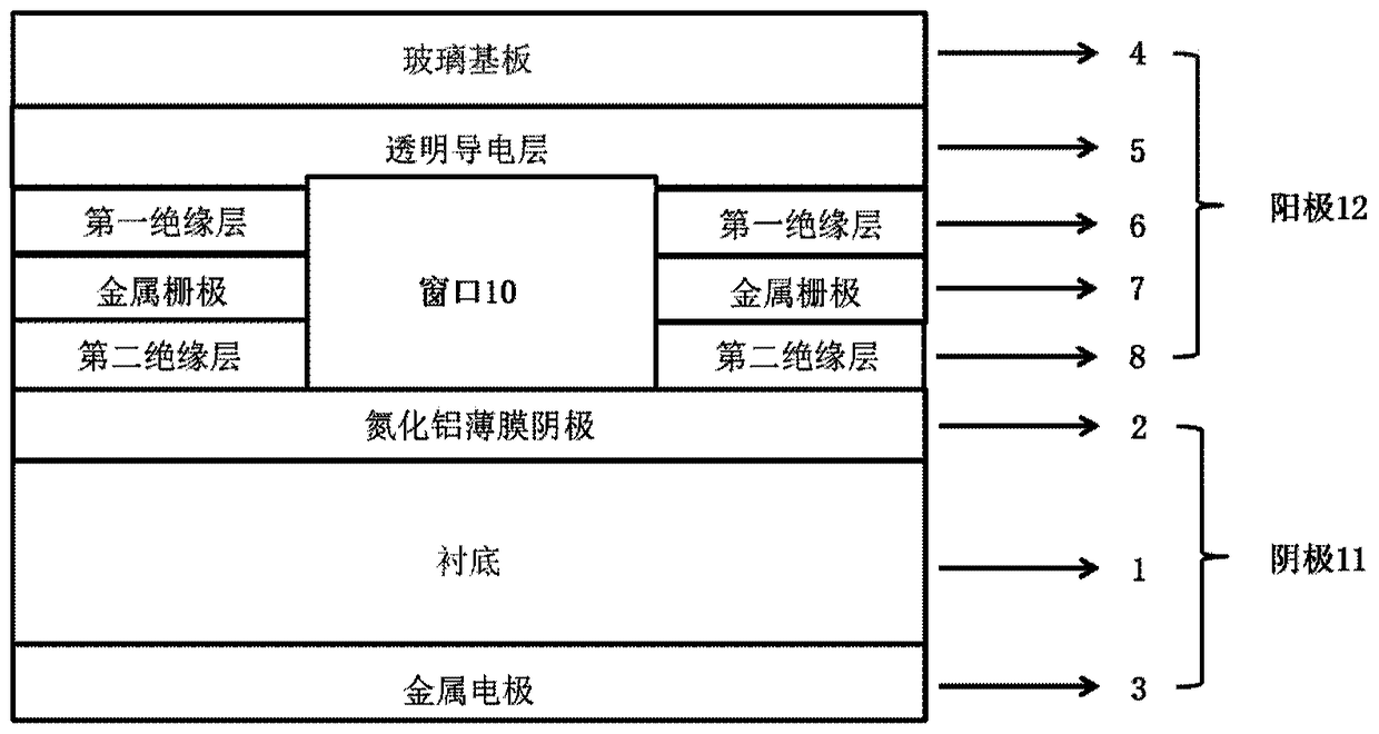
[0030] see figure 1 As shown, the present invention provides a nano-vacuum triode structure with an inverted anode, comprising:

[0031] A substrate 1, which can be semi-insulating sapphire or silicon carbide, with a resistivity of 0.03-0.04Ω·cm and a thickness of 300-450μm;

[0032] An aluminum nitride thin film cathode 2, the aluminum nitride thin film cathode 2 is grown on the front side of the substrate 1 by MOCVD method, the aluminum nitride thin film cathode 2 is doped with n-type Si, and the Si doping concentration is 1×10 18 cm -3 -1×10 21 cm -3 , the thickness is 50nm-500nm;

[0033] A metal electrode 3, the metal electrode 3 is made on the back of the substrate 1, and a layer of Ni / Au alloy is first made on the back of the substrate 1 by PECVD or sputtering method, and the Ni / Au alloy is formed with the substrate 1 after annealing Good ohmic contact, the thickness of Ni and Au is divided into 50nm and 50nm, the annealing temperature is 950°C-1050°C, the annealin...


PUM

PropertyMeasurementUnit
thicknessaaaaaaaaaa
thicknessaaaaaaaaaa
thicknessaaaaaaaaaa

Abstract

Provided is a nanometer vacuum triode structure with a flip-chip-type anode, comprising a substrate; an aluminum nitride film cathode growing on the front side of the substrate; a metal electrode manufactured on the back of the substrate, wherein the substrate, the aluminum nitride film cathode and the metal electrode form a cathode; a glass substrate; a transparent conducting layer manufactured on the glass substrate; a first insulating layer manufactured on the transparent conducting layer, wherein the intermediate part is a window; a metal gate manufactured on the first insulating layer, wherein the intermediate part is a window; and a second insulating layer manufactured on the metal gate, wherein the intermediate part is a window, and the glass substrate, the transparent conducting layer, the first insulating layer, the metal gate and the second insulating layer form an anode. The second insulating layer of the cathode and the aluminum nitride film cathode of the cathode are in buckled connection to form a nanometer vacuum triode structure with a flip-chip-type anode. The nanometer vacuum triode structure with a flip-chip-type anode overcomes deficiencies of a present nanometer vacuum triode structure, and can avoid cathode oxidation, improve the electronic collection capability of the anode, and facilitate flip-chip integration.

Description

technical field [0001] The invention belongs to the field of field emission electronic devices in the vacuum electron technology, and in particular relates to a nanometer vacuum triode structure and a preparation method of an inverted anode. Background technique [0002] In the past ten years, Group III nitride materials have shown excellent characteristics in the field of optoelectronic and microelectronic devices such as solid-state light-emitting diodes, blue / green lasers, high electron mobility transistors and solar cells, and their related devices have been researched by countries all over the world. Institutional attention and extensive research. Aluminum nitride is one of the representatives, and its unique negative electron affinity makes it a new research hotspot in the field of vacuum microelectronics. For materials with negative electron affinity, since the binding of electrons on the surface is almost zero, when a small voltage is applied, considering the suffic...

Claims


Application Information

Patent Timeline
Patent Type & Authority Patents(China)
IPC IPC(8): H01J21/10H01J19/32H01J9/00
Inventor 梁锋陈平赵德刚侍铭刘宗顺江德生
Owner INST OF SEMICONDUCTORS - CHINESE ACAD OF SCI
Why Eureka
Try Eureka