Method for manufacturing soldering circuit board, soldering circuit board, and method for mounting electronic component

A technology of solder circuit substrate and manufacturing method, applied in the direction of printed circuit manufacturing, circuit, printed circuit, etc., to achieve the effect of expanding the range of choices

Inactive Publication Date: 2015-12-02
SHOWA DENKO KK
View PDF4 Cites 3 Cited by
  • Summary
  • Abstract
  • Description
  • Claims
  • Application Information

AI Technical Summary

Problems solved by technology

If the thickness of the solder layer of the soldered circuit board varies due to this, there will be adverse effects such as variation in the bonding strength between t

Method used


Image

  • Method for manufacturing soldering circuit board, soldering circuit board, and method for mounting electronic component
  • Method for manufacturing soldering circuit board, soldering circuit board, and method for mounting electronic component
  • Method for manufacturing soldering circuit board, soldering circuit board, and method for mounting electronic component

Examples


Embodiment 1

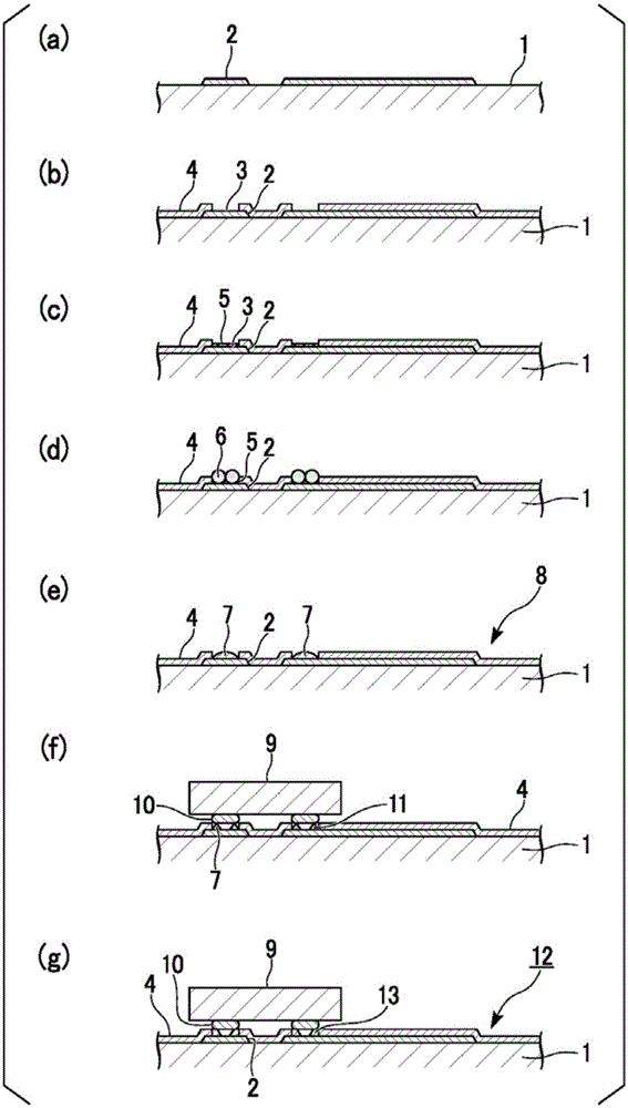
[0105] Copper was used as a conductive substance to produce a printed wiring board (hereinafter simply referred to as "printed wiring board"). The line width of the circuit pattern of the printed wiring board made of the conductive material was 25 μm, and the space between the narrowest circuit patterns was 25 μm. A substrate in which a photoresist (model: H-7034, manufactured by Hitachi Chemical Co., Ltd.) was attached to the printed wiring board was prepared. After exposing the printed wiring board to ultraviolet rays using a photomask, the printed wiring board is patterned using an alkaline developing solution such as a 1% sodium carbonate aqueous solution. In the region not covered with the resist on the surface of the conductive circuit electrode, the size was set to 25×80 μm every other electrode.

[0106] As the tackiness-imparting compound solution, the alkyl group of R12 of the general formula (3) was changed to C by using acetic acid. 11 h 23 , a solution in which...

Embodiment 2

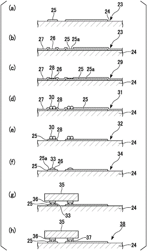
[0110] A bare chip was mounted on a printed wiring board in the same steps and conditions as in Example 1, except that the heating of the printed wiring board after solder powder adhesion was not performed (second heating step).


PUM

PropertyMeasurementUnit
Line widthaaaaaaaaaa

Abstract

The present invention is a method for manufacturing a soldering circuit board and is characterized by carrying out in this order: a resist forming step for partially covering a conductive circuit electrode surface on a printed wiring board with a resist; an adhering part forming step that forms an adhering part by imparting adhesiveness to parts that are not covered by the resist on the conductive circuit electrode surface; a solder attachment step for attaching solder powder to the adhering part; a resist removal step for removing the resist; and a first heating step that heats the printed wiring board and melts the solder powder.

Description

technical field [0001] The present invention relates to a method for manufacturing a solder (solder) circuit board, and a method for mounting a solder circuit board and electronic components. this application claims the priority based on the patent application 2013-081208 for which it applied to Japan on April 9, 2013, The content is used here. Background technique [0002] In recent years, electronic circuits in which electronic components such as IC elements and semiconductor chips are solder-bonded to a circuit pattern have been put into practical use. The circuit pattern is formed on a plastic substrate, a ceramic substrate, or an insulating substrate coated with plastic or the like. [0003] The following methods are known as methods for bonding lead terminals of electronic components to predetermined portions of circuit patterns when manufacturing such electronic circuits. For example, it is known that a solder layer is previously formed on the surface of a conductiv...

Claims


Application Information

Patent Timeline
IPC IPC(8): H05K3/34H01L21/60
CPCH05K3/3484H01L21/4853H01L23/49811H01L24/13H01L24/81H01L2224/03442H01L2224/0347H01L2224/03849H01L2224/0401H01L2224/1134H01L2224/81075H01L2224/81191H01L2224/8121H01L2224/8123H01L2224/8138H01L2224/814H01L2224/81409H01L2224/81411H01L2224/81413H01L2224/81416H01L2224/81444H01L2224/81815H01L2924/01322H01L2924/15787H01L2924/3841H05K3/3436H05K2203/0425H01L2924/351H01L2924/381H05K3/3452H05K3/3489H05K2203/043H05K2203/0568H05K2203/0769H05K2203/0776H05K2203/0789H05K2203/124H05K3/3463H05K3/3485H01L2924/01082H01L2924/01047H01L2924/0105H01L2924/01083H01L2924/01048H01L2924/01049H01L2924/0103H01L2924/01029H01L2924/01051H01L2924/01079H01L2924/01032H01L2924/014H01L2924/00014H01L2924/00012H01L2924/00H05K3/3494
Inventor 堺丈和
Owner SHOWA DENKO KK
Why Eureka
Try Eureka