Method for controlling the density of sic nanoarrays

A nano-array and density technology, applied in nanotechnology, nanotechnology, chemical instruments and methods, etc., can solve the problems of restricting the growth direction of products, expensive carbon nanotubes, and self-consumption, etc., and achieves easy industrial production and distribution density. and size-effective, cost-effective

Active Publication Date: 2016-11-02
NINGBO UNIVERSITY OF TECHNOLOGY
View PDF8 Cites 2 Cited by
  • Summary
  • Abstract
  • Description
  • Claims
  • Application Information

AI Technical Summary

Problems solved by technology

On the one hand, it provides the required carbon source in the reaction and consumes itself; on the other hand, carbon nanotubes provide a nucleation site while limiting the growth direction of the product
However, carbon nanotubes are relatively expensive, so the cost of carbon nanotube template method is very high

Method used


Image

  • Method for controlling the density of sic nanoarrays
  • Method for controlling the density of sic nanoarrays
  • Method for controlling the density of sic nanoarrays

Examples


Embodiment 1

[0042] In this embodiment, the SiC nano-array includes a substrate and a nano-array formed on the surface of the substrate,

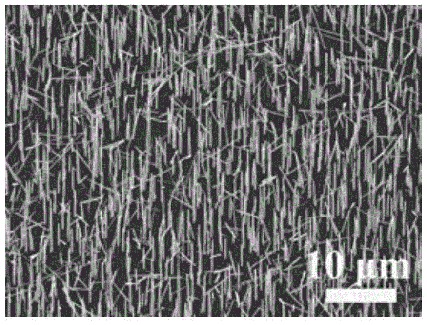
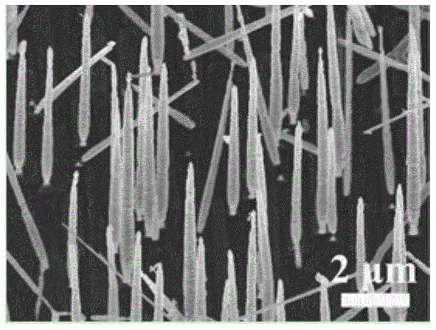
[0043] The nanoarray is an arrangement of SiC nanowires, wherein the SiC crystal form in the SiC nanowires is C type, H type or R type; the SiC nanowires are needle-like structures with a thick bottom and a thin top (SiC nanowires can also be a linear structure)

[0044] The array density of nanowires in SiC nanoarrays is (5.0-6.0)×10 7 root / cm 2 (Preferably (5.2-5.7)×10 7 root / cm 2 ).

Embodiment 2

[0046] In this embodiment, the SiC nano-array includes a substrate and a nano-array formed on the surface of the substrate. The substrate is a SiC substrate, and the lattice structure of the SiC substrate includes 3C-SiC, 2H-SiC, 4H-SiC, 6H-SiC, 15R- Any of SiC;

[0047] The nanoarray is an arrangement of SiC nanowires, wherein the SiC crystal form in the SiC nanowires is C type, H type or R type; the SiC nanowires are needle-like structures with a thick bottom and a thin top (SiC nanowires can also be a linear structure)

[0048] The array density of nanowires in SiC nanoarrays is (5.0-6.0)×10 7 root / cm 2 .

Embodiment 3

[0050] In this embodiment, the SiC nano-array includes a substrate and a nano-array formed on the surface of the substrate. The substrate is a SiC substrate, and the lattice structure of the SiC substrate includes 3C-SiC, 2H-SiC, 4H-SiC, 6H-SiC, 15R- Any of SiC;

[0051] The nano-array is an arrangement of SiC nanowires, wherein the SiC crystal type in the SiC nanowires is C-type, H-type or R-type; the SiC nanowires have a needle-like structure with a thick bottom and a thin top (SiC nanowires can also be a linear structure), When SiC crystal form in SiC nanowire is C type, SiC is 3C-SiC; when SiC crystal form in SiC nanowire is H type, SiC is any of 2H-SiC, 4H-SiC, 6H-SiC; in SiC nanowire, SiC When the crystal form is R type, SiC is 15R-SiC;

[0052] The array density of nanowires in SiC nanoarrays is (5.0-6.0)×10 7 root / cm 2 .


PUM

PropertyMeasurementUnit
thicknessaaaaaaaaaa
thicknessaaaaaaaaaa
thicknessaaaaaaaaaa

Abstract

The invention discloses a method of regulating and controlling density of a SiC nano array, which includes following steps: 1) preparation of a precursor and a substrate; 2) catalyst deposition: depositing a catalyst layer on the surface of a substrate; and 3) sintering: sintering the substrate deposited with the catalyst layer and the precursor under a sintering atmosphere, so that the precursor is pyrolyzed on the surface of the substrate to form the SiC nano array. The preparation method is simple in process, is convenient to carry out, is beneficial to scale enlargement, is good in safety, is good in product quality stability and is stable in product performance.

Description

technical field [0001] The invention relates to a method for preparing an inorganic semiconductor material, in particular to a method for regulating and controlling the density of SiC nanometer arrays. Background technique [0002] Silicon carbide (SiC) is one of the core materials of third-generation semiconductors, and it has many advantages compared with elemental semiconductor materials (Si) and other compound semiconductor materials GaAs, GaP and InP. Silicon carbide not only has a large bandgap width (the bandgap widths of 3C, 4H, and 6H types of silicon carbide at room temperature are 2.23, 3.22, and 2.86eV, respectively), but also has a high critical breakdown electric field, high thermal conductivity, and high load. Drift speed and other characteristics of the carrier have great application prospects in high temperature, high frequency, high power, optoelectronics and radiation resistance. Replacing silicon with silicon carbide to prepare optoelectronic devices and...

Claims


Application Information

Patent Timeline
Patent Type & Authority Patents(China)
IPC IPC(8): C30B29/36C30B1/00H01J1/304C01B31/36B82Y30/00
Inventor 王霖陈善亮杨为佑
Owner NINGBO UNIVERSITY OF TECHNOLOGY
Why Eureka
Try Eureka