Packaging structure and manufacturing method for redistribution leading wire layer
A technology for redistribution leads and manufacturing methods, which is applied in semiconductor/solid-state device manufacturing, electrical components, electric solid-state devices, etc., can solve the problems of complex manufacturing process of redistribution lead layer, insufficient environmental protection, low production efficiency, etc., and achieve reduction in process Complexity, avoidance of risk of damage, effect of saving material
- Summary
- Abstract
- Description
- Claims
- Application Information
AI Technical Summary
Problems solved by technology
Method used
Image

Examples
Embodiment 1
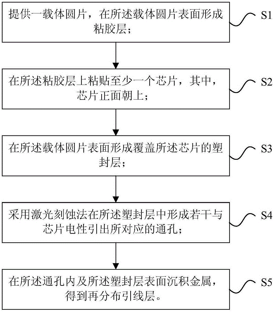
[0067] The present invention provides a manufacturing method of redistribution lead layer, please refer to figure 1 , shown as a process flow diagram of the method, comprising the following steps:
[0068] S1: providing a carrier, forming an adhesive layer on the surface of the carrier;
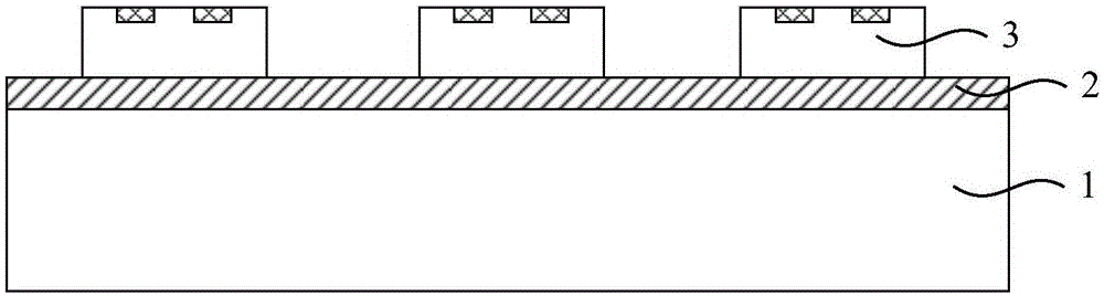
[0069] S2: Paste at least one chip on the adhesive layer, wherein the chip faces upward;
[0070] S3: forming a plastic encapsulation layer covering the chip on the surface of the carrier;
[0071] S4: Forming several through holes corresponding to the electrical leads of the chip in the plastic encapsulation layer by laser etching;
[0072] S5: Depositing metal in the through hole and on the surface of the plastic encapsulation layer to obtain a redistribution wiring layer.
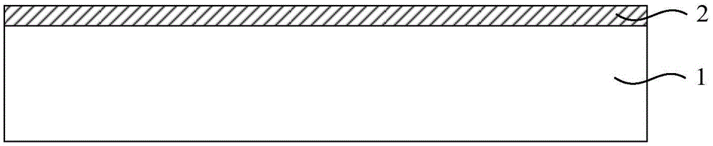
[0073] See first figure 2 , performing step S1: providing a carrier 1, and forming an adhesive layer 2 on the surface of the carrier 1.
[0074] Specifically, the function of the carrier 1 is to provide a rigid st...
Embodiment 2
[0098] This embodiment adopts basically the same technical solution as Embodiment 1. The difference is that in Embodiment 1, only laser etching is used to form through holes in the plastic packaging layer, and finally the metal lines of the redistribution lead layer are formed in the plastic packaging layer. In this embodiment, the redistribution lead layer pattern (including through holes and metal circuit patterns) is formed in the plastic encapsulation layer by laser etching, and then the metal deposition process is used to form the redistribution lead layer composed of metal and metal lines in the through holes. The lead layer is distributed, and finally the metal circuit of the redistributed lead layer is embedded in the plastic sealing layer, which has higher reliability.
[0099] See first Figure 2 to Figure 4 , performing steps S1 to S3 that are basically the same as those in Embodiment 1.
[0100] then see Figure 5 and Figure 12 , performing step S4: using laser...
Embodiment 3
[0119] This embodiment adopts basically the same technical solution as that of Embodiment 2, except that in this embodiment, the redistribution wiring layer is obtained by laser direct forming.
[0120] Laser Direct Structuring (LDS) is a method of creating electronic circuits on injection-molded plastic parts using steps such as laser ablation and metallization. The laser direct molding method usually includes the following steps: (1) Injection molding (Injection molding), which is automatically formed after the molten plastic is sprayed out by a plastic injection machine. (2) Laser Activation (Laser Activation), this step uses the computer to control the movement of the laser according to the trajectory of the conductive pattern, projects the laser onto the molded three-dimensional plastic device, and activates the circuit pattern within a few seconds. In this process, the laser energy breaks the organic coating surrounding the metal particles on the one hand, exposing the m...
PUM
 Abstract
Description
Claims
Application Information
 - R&D
- Intellectual Property
- Life Sciences
- Materials
- Tech Scout
- Unparalleled Data Quality
- Higher Quality Content
- 60% Fewer Hallucinations
Browse by: Latest US Patents, China's latest patents, Technical Efficacy Thesaurus, Application Domain, Technology Topic, Popular Technical Reports.
© 2025 PatSnap. All rights reserved.Legal|Privacy policy|Modern Slavery Act Transparency Statement|Sitemap|About US| Contact US: help@patsnap.com