Manufacturing method of array substrate

A manufacturing method and array substrate technology, applied in the direction of electrical components, electrical solid devices, circuits, etc., can solve the problems of TET characteristic changes, pollution, and affecting the display effect of the display, and achieve the effect of guaranteeing the characteristics

Inactive Publication Date: 2015-12-09
TCL CHINA STAR OPTOELECTRONICS TECH CO LTD
View PDF3 Cites 3 Cited by
  • Summary
  • Abstract
  • Description
  • Claims
  • Application Information

AI Technical Summary

Problems solved by technology

[0012] The invention provides a method for manufacturing an array substrate, which can solve the problem in the prior art that the pollution of the channel semiconductor caused by Cu metal diffusion in the source and drain electrodes changes the TET characteristics and affects the display effect of the display.

Method used


Image

  • Manufacturing method of array substrate
  • Manufacturing method of array substrate
  • Manufacturing method of array substrate

Examples


Embodiment Construction

[0044] The present invention will be described in detail below in conjunction with the accompanying drawings and specific embodiments.

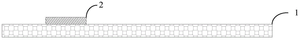
[0045] refer to Figure 7 , is a schematic flowchart of a first embodiment of a method for fabricating an array substrate according to the present invention.

[0046] A method for manufacturing an array substrate provided by the present invention, the method includes the following steps:

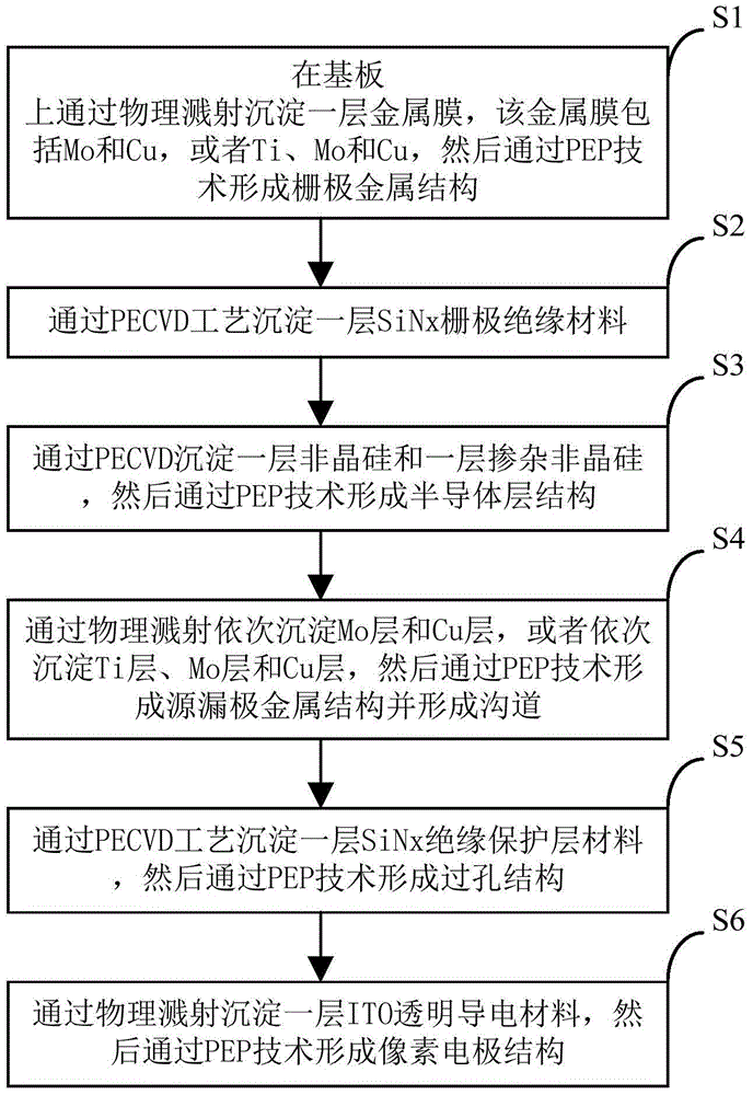
[0047] S100, forming a gate metal structure 200 on the substrate 100, such as Figure 8 shown.

[0048] Wherein, the substrate 100 may be quartz glass, common glass, plastic substrate and so on. The gate metal structure 200 is a metal film deposited by physical sputtering, the metal film at least includes a Mo layer and a Cu layer, wherein the thickness of the Mo layer is 100A-300A, for example, 150A, 200A or 250A. The thickness of the Cu layer is about 3000A-6000A, such as 3500A, 4000A or 5000A. Alternatively, the metal film may also include a metal Ti ...


PUM


Abstract

The invention provides a manufacturing method of an array substrate. The method comprises the following steps: forming a gate metal structure on a substrate; forming a gate insulating layer on the gate metal structure; forming a semiconductor structure on the gate insulating layer and forming a channel; forming a metal structure having source and drain electrodes on the semiconductor structure; forming an insulating protection layer on the source and drain electrodes, and forming a via hole on the insulating protection layer; and forming a pixel electrode on the insulating protection layer. In the manner, the phenomenon that a channel semiconductor is polluted by Cu metal oxidation and diffusion can be avoided, so that the characteristics of a thin film transistor (TFT) can be ensured, and the display effect of a display is not affected.

Description

technical field [0001] The present invention relates to the field of display technology, in particular to a method for manufacturing an array substrate. Background technique [0002] With the development of flat panel display (FPD) technology, people's pursuit of display resolution and frame refresh rate is getting higher and higher, so the development of new materials and new processes is imminent. At present, in the field of TFT-LCD, aluminum and molybdenum are the main metal materials for the conductive layer. The advantages of aluminum and molybdenum are that the film forming process is simple, the adhesion and flatness are good, and the softness is not easy to cause climbing and disconnection, and it is not easy to Diffusion (membrane contamination). Aluminum is the ideal conductive metal material of choice for small size and low resolution panels. Since the resistivity of aluminum is relatively large, it cannot meet the demand for large size and high resolution. As ...

Claims


Application Information

Patent Timeline
IPC IPC(8): H01L27/12
Inventor 徐向阳
Owner TCL CHINA STAR OPTOELECTRONICS TECH CO LTD
Why Eureka
Try Eureka