GaN-based light emitting diode (LED) array micro display device and fabrication method thereof

A technology for LED arrays and micro-display devices, applied in the direction of electric solid devices, semiconductor devices, electrical components, etc., can solve the problems of resolution limitation, affecting device luminous efficiency, micro-LED chip lattice damage, etc., and achieve ultra-high resolution , the effect of low leakage current and ultra-low power consumption

Active Publication Date: 2015-12-09
SUN YAT SEN UNIV
View PDF6 Cites 4 Cited by
  • Summary
  • Abstract
  • Description
  • Claims
  • Application Information

AI Technical Summary

Problems solved by technology

Limited by the precision of the ICP etching process, it is difficult to make the size of the light-emitting pixel of the display device made by this method smaller, so the resolution is limited to a certain extent, and it does not meet the development nee

Method used


Image

  • GaN-based light emitting diode (LED) array micro display device and fabrication method thereof
  • GaN-based light emitting diode (LED) array micro display device and fabrication method thereof
  • GaN-based light emitting diode (LED) array micro display device and fabrication method thereof

Examples


Embodiment 1

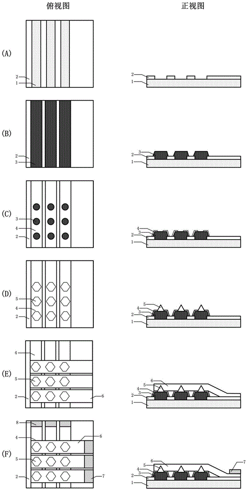
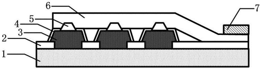
[0033] attached figure 1 Among them, 1-sapphire substrate, 2-masking film arranged in stripes, 3-striped n-type GaN array, 4-masking film with periodically arranged holes, 5-micro LED array in pyramid structure, 6- Strip-shaped transparent conductive layer, 7-positive electrode, 8-negative electrode.

[0034] Such as figure 1 As shown, a method for preparing a GaN-based LED array microdisplay device based on selective area epitaxial growth technology is provided, which includes the following steps:

[0035] (A): 100nm thick SiO deposited on sapphire substrate 2 Dielectric masking film, the SiO 2 The dielectric masking film is prepared as a masking film arranged in strips with a window area width of 10 μm and an interval of 5 μm;

[0036] (B): The selective area epitaxial growth technique by MOCVD, in the above SiO with stripe arrangement 2 Epitaxial growth of strip-structured n-type GaN arrays on the window region of the masking film;

[0037] (C): Deposition of 100nm th...

Embodiment 2

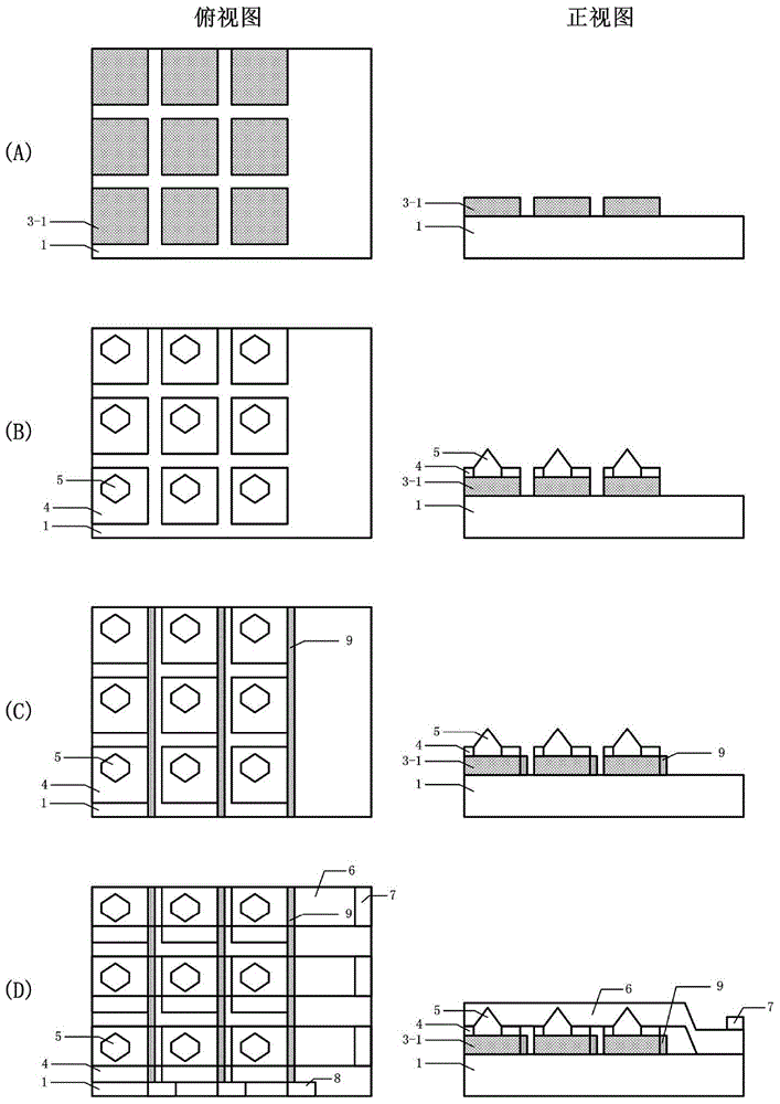
[0043] attached figure 2 Among them, 1-sapphire substrate, 3-1-n-type GaN epitaxial layer, 4-masking film with periodically arranged holes, 5-pyramid structure micro LED array, 6-strip transparent conductive layer, 7-positive Electrode, 8-negative electrode, 9-column interconnected conductive layer.

[0044] Such as figure 2 As shown, a method for preparing a GaN-based LED array microdisplay device based on selective area epitaxial growth technology is provided, which includes the following steps:

[0045] (A) An n-type GaN epitaxial layer with a thickness of 2 μm is grown on a sapphire substrate by MOCVD epitaxy, and the n-type GaN epitaxial layer is etched into an array of isolated blocks by ICP dry etching Shaped n-type GaN epitaxial layer, the size of each block n-type GaN epitaxial layer is 12x12 μm, and the interval between each other is 3 μm;

[0046] (B) On each bulk n-type GaN epitaxial layer, a masking film with periodically arranged openings is made, and at the...

Embodiment 3

[0050] Embodiment 3 adopts the same epitaxial structure, device structure and manufacturing process as Embodiment 1, wherein the pyramidal micro LED array in Embodiment 1 is replaced by the hexagonal truncated pyramid micro LED array in Embodiment 3.


PUM

PropertyMeasurementUnit
Bar widthaaaaaaaaaa
Diameteraaaaaaaaaa
Thicknessaaaaaaaaaa

Abstract

The invention discloses a GaN-based light emitting diode (LED) array micro display device and a fabrication method thereof based on a selective region epitaxial growth technique. The fabrication method of the device comprises the following steps of: (A) fabricating mask membranes arranged in a strip shape on a substrate, and growing a strip-structurized n-type GaN array through the selective region epitaxial growth technique; (B) fabricating a mask membrane provided with periodically-distributed opening holes on the strip-structurized n-type GaN array, and growing a three-dimensional structurized miniature LED array through the selective region epitaxial growth technique; (C) fabricating a strip-shaped transparent conductive layer on the surface of the three-dimensional structurized miniature LED array; and (D) respectively fabricating a negative electrode and a positive electrode on the strip-structurized n-type GaN array and the strip-shaped transparent conductive layer. According to the method, the selective region epitaxial growth technique is used for growing a GaN-based miniature LED, the problem of current leakage caused by a dry etching method for fabrication the miniature LED is solved, and a miniature display device having matrix addressing, low power consumption and high brightness is provided.

Description

technical field [0001] The invention belongs to the field of semiconductor light emitting devices, relates to a micro display device, in particular to a GaN-based LED array micro display device based on selective area epitaxial growth technology and a manufacturing method thereof. Background technique [0002] Group III nitrides GaN, AlN (bandgap 6.2eV), InN (bandgap 0.7eV) and their alloys cover the energy range from infrared to visible light and ultraviolet light, so they are used in semiconductor light-emitting devices. The field has a wide range of applications. In recent years, with the development of the electronics industry and the advancement of industrial technology, micro-light-emitting devices based on group-III nitrides have developed rapidly, opening up new application fields for group-III nitride-based light-emitting devices. [0003] At present, micro-display devices have become the focus of attention of various countries by virtue of their unique advantage...

Claims


Application Information

Patent Timeline
IPC IPC(8): H01L33/00H01L33/20H01L27/15
CPCH01L27/153H01L33/007H01L33/20
Inventor 张佰君陈伟杰
Owner SUN YAT SEN UNIV
Why Eureka
Try Eureka