Organic light emitting diode (OLED) display panel, preparation method thereof and display device

An electroluminescence display and display panel technology, which is applied in the direction of circuits, electrical components, and electric solid-state devices, and can solve problems such as low product resolution and complex manufacturing process of OLED display panels

Active Publication Date: 2015-12-16
BOE TECH GRP CO LTD
View PDF3 Cites 28 Cited by
  • Summary
  • Abstract
  • Description
  • Claims
  • Application Information

AI Technical Summary

Problems solved by technology

[0005] Embodiments of the present invention provide an organic electroluminescent display panel, its preparation method, and a display device, which are used to ...

Method used


Image

  • Organic light emitting diode (OLED) display panel, preparation method thereof and display device
  • Organic light emitting diode (OLED) display panel, preparation method thereof and display device
  • Organic light emitting diode (OLED) display panel, preparation method thereof and display device

Examples


preparation example Construction

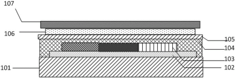
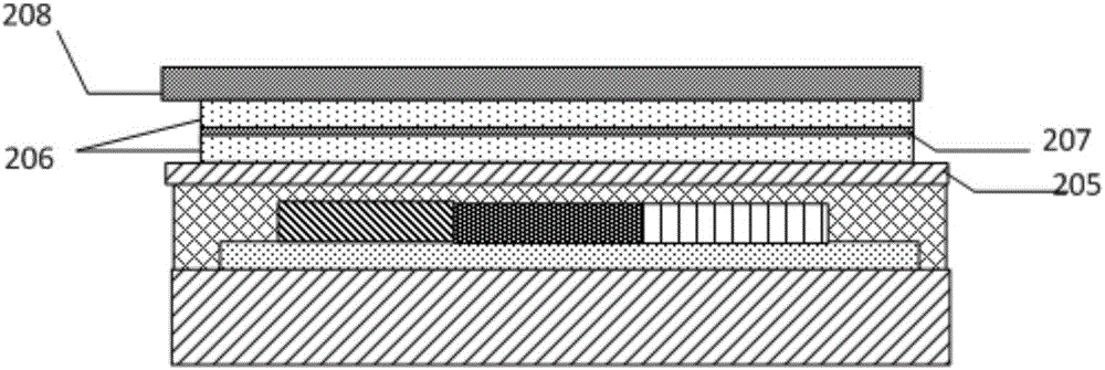
[0063] Based on the same inventive concept, an embodiment of the present invention provides a method for preparing an organic electroluminescent display panel, such as Figure 8 As shown, the following steps may be specifically included:

[0064] S101, forming a switching transistor array on a flexible substrate through a patterning process;

[0065] S102, forming a white organic light emitting diode on the flexible substrate formed with the switch transistor array;

[0066] S103, performing a thin film packaging process on the flexible substrate formed with white organic light emitting diodes to form a first packaging film;

[0067] S104, forming metal color filters with periodic nanostructures on the flexible substrate formed with the first encapsulation film by photolithography;

[0068] S105 , performing a thin film packaging process on the flexible substrate on which the metal color filter is formed, to form a second packaging film.

[0069] In the method for preparing...


PUM

PropertyMeasurementUnit
Thicknessaaaaaaaaaa

Abstract

The invention discloses an organic light emitting diode (OLED) display panel, a preparation method thereof and a display device. The organic light emitting diode display panel comprises a white organic light-emitting diode and a metal color filter of a period nanostructure. By arranging a layer of the metal color filter of the period nanostructure to be integrated with a backlight source of the white organic light-emitting diode, a color OLED display structure can be achieved. Compared with the conventional OLED color display structure, the organic light emitting diode display panel provided by an embodiment of the invention only uses one manufacturing process to form the metal color filter. Compared with that a RGB color film layer by more than once evaporation technology in the prior art, the invention can reduce the mask number, simplify the manufacturing technology of the OLED display panel and reduce the production cost. In addition, the metal color filter of the period nanostructure is used for facilitating development of high-resolution products.

Description

technical field [0001] The invention relates to the field of display technology, in particular to an organic electroluminescence display panel, a preparation method thereof and a display device. Background technique [0002] With the advancement of display technology, organic electroluminescent display (OrganicLightEmittingDiode, OLED) is one of the hotspots in the field of flat panel display research today, and more and more active matrix organic light emitting diode (ActiveMatrixOrganicLightEmittingDiode, AMOLED) display panels have entered the market, relatively Compared with the traditional thin film transistor liquid crystal display panel (ThinFilmTransistorLiquidCrystalDisplay, TFTLCD), AMOLED has faster response speed, higher contrast ratio and wider viewing angle. [0003] The structure of the traditional top-emitting OLED display panel is as follows: figure 1 As shown, it mainly includes: flexible substrate 101, switching transistor array 102, RGB color filter laye...

Claims


Application Information

Patent Timeline
IPC IPC(8): H01L27/32H01L51/52H01L51/56
CPCH10K59/12H10K50/84H10K71/00
Inventor 刘震毛雪
Owner BOE TECH GRP CO LTD
Why Eureka
Try Eureka