Transverse high-pressure device and manufacturing method thereof

A lateral high-voltage, device technology, used in semiconductor/solid-state device manufacturing, semiconductor devices, electrical components, etc., can solve problems such as rising on-resistance and limiting applications

Inactive Publication Date: 2015-12-16
UNIV OF ELECTRONICS SCI & TECH OF CHINA
View PDF6 Cites 6 Cited by
  • Summary
  • Abstract
  • Description
  • Claims
  • Application Information

AI Technical Summary

Problems solved by technology

When the device is used in high-voltage applications, the on-resistance rises sharply, which limits the application of high-voltage devices in high-voltage power integrated circuits, especially circuits that require low conduction loss and small chip area
In order to overcome the problem of high on-resistan

Method used


Image

  • Transverse high-pressure device and manufacturing method thereof
  • Transverse high-pressure device and manufacturing method thereof
  • Transverse high-pressure device and manufacturing method thereof

Examples


Embodiment 1

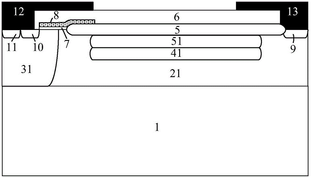
[0041] figure 2 A cross-sectional view of a lateral high-voltage device structure provided in this embodiment.

[0042] A lateral high-voltage device, the cell structure of which includes a first conductivity type semiconductor substrate 1, a second conductivity type semiconductor drift region disposed above the first conductivity type semiconductor substrate 1, and the second conductivity type semiconductor drift region is composed of A plurality of semiconductor sub-drift regions 21, 22...2i of the second conductivity type are stacked sequentially from bottom to top, and each semiconductor sub-drift region of the second conductivity type includes: one located on the left side of the semiconductor sub-drift region of the second conductivity type The first conductivity type semiconductor body region, one first conductivity type semiconductor drop field layer arranged on the right side of the first conductivity type semiconductor body region, one first conductivity type semico...

Embodiment 2

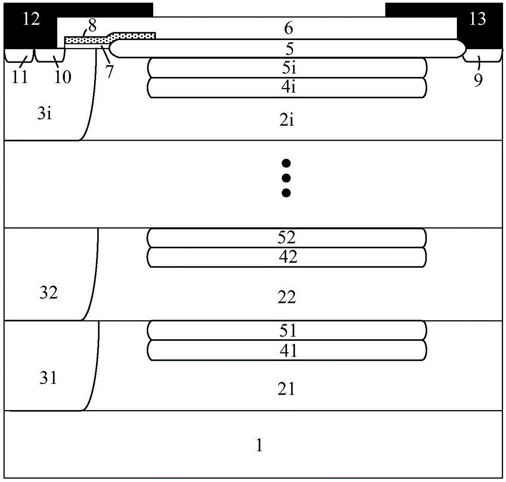
[0045] Such as image 3 As shown, the difference between this embodiment and Embodiment 1 is that: not every semiconductor sub-drift region 21, 22...2i of the second conductivity type is provided with a second conductivity type semiconductor heavily doped layer; the second conductivity type The i-th heavily doped semiconductor layer is disposed on the upper surface of the i-th drift region of the uppermost second-conductivity-type semiconductor and above the i-th drop field layer of the first-conduction-type semiconductor in the i-th drift region.

Embodiment 3

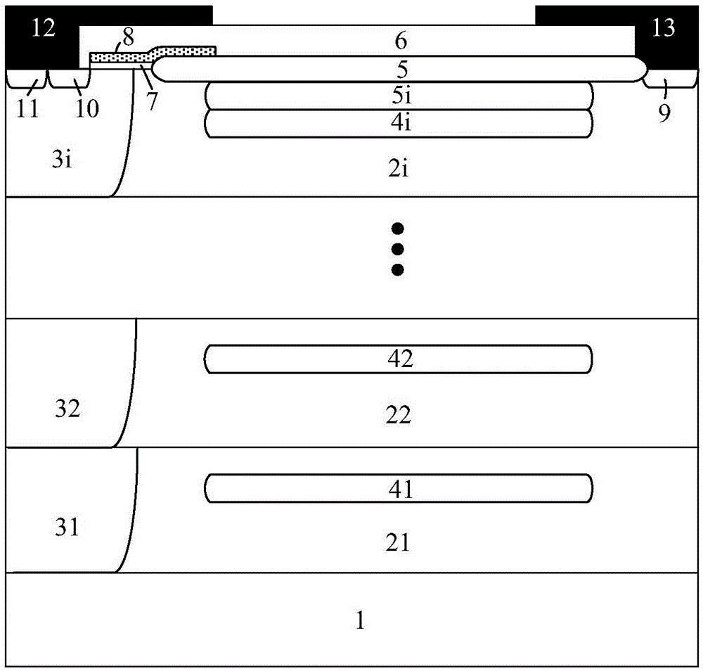
[0047] Such as Figure 4 As shown, this embodiment is basically the same as Embodiment 1, the difference is that it also includes a buried oxide layer 2, and the buried oxide layer 2 is arranged on the semiconductor substrate 1 of the first conductivity type and the first drift region 21 of the semiconductor of the second conductivity type. The device is integrated on the SOI substrate, and its working principle and effect are the same as those in Embodiment 1.


PUM

PropertyMeasurementUnit
Thicknessaaaaaaaaaa

Abstract

The invention provides a transverse high-pressure device and a manufacturing method thereof. A cellular structure of the device comprises a first conductive-type semiconductor substrate and second conductive-type semiconductor drift regions. The plurality of second conductive-type semiconductor drift regions are laminated from down to up in sequence. The method comprises the steps of: adopting an epitaxial technology to successively form the second conductive-type semiconductor drift regions; forming a first conductive-type semiconductor reduced-field layer, a second conductive-type semiconductor heavily doped layer and a first conductive-type semiconductor body region in each second conductive-type semiconductor drift region in an injecting manner. According to the invention, a conventional drift region structure is made into a drift region structure with a plurality of layers of superposed drift regions, so that each sub drift region is provided with a low-resistance nearest conductive path, and the conduction resistance of the device is lowered; and in an off state, the reduced-field layer in each drift region assists to consume the drift region, so that the breakdown voltage of the device is increased, and the contradiction relation between the conduction resistance and a withstand voltage is relieved.

Description

technical field [0001] The invention relates to the technical field of semiconductor power devices, and relates to a lateral high voltage device and a manufacturing method thereof. Background technique [0002] Lateral high-voltage devices are an essential part of the development of high-voltage power integrated circuits. High-voltage power devices require high breakdown voltage, low on-resistance and low switching loss. To achieve a high breakdown voltage of a lateral high voltage device, the drift region used to withstand the voltage is required to have a long size and low doping concentration, but in order to meet the low on-resistance of the device, the drift region as a current channel is required to have a high doping concentration. In the design of power LDMOS (LatralDouble-diffusedMOSFET) devices, breakdown voltage (BreakdownVoltage, BV) and specific on-resistance (Specificon-resistance, R on,sp ) has a contradictory relationship. When the device is used in high-v...

Claims


Application Information

Patent Timeline
IPC IPC(8): H01L29/78H01L29/06H01L21/336
CPCH01L29/7835H01L29/0611H01L29/0684H01L29/66659
Inventor 乔明王裕如代刚周锌何逸涛张波
Owner UNIV OF ELECTRONICS SCI & TECH OF CHINA
Why Eureka
Try Eureka