Pixel circuit for three-dimensional imaging chip

A pixel circuit and three-dimensional imaging technology, applied in the field of pixel circuits, can solve the problem of low energy of a single photon, achieve the effects of enhancing detection sensitivity, reducing processing time, and increasing application value

Inactive Publication Date: 2015-12-23
XIANGTAN UNIV
View PDF4 Cites 6 Cited by
  • Summary
  • Abstract
  • Description
  • Claims
  • Application Information

AI Technical Summary

Problems solved by technology

Due to the extremely low energy of a single photon, it is difficult

Method used


Image

  • Pixel circuit for three-dimensional imaging chip
  • Pixel circuit for three-dimensional imaging chip
  • Pixel circuit for three-dimensional imaging chip

Examples


Embodiment Construction

[0017] The present invention will be described in further detail below in conjunction with accompanying drawing.

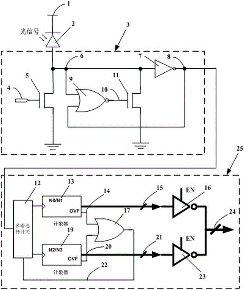
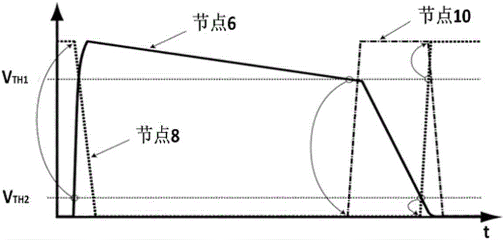
[0018] see figure 1 , the present invention includes single photon avalanche diode 2, passive quenching and active recharging circuit 3, multiplex switch 12, or gate 17, two counters (13,19), two groups of tri-state gate switches (16,23 ); a reverse bias voltage higher than its avalanche breakdown voltage is applied to both ends of the single photon avalanche diode 2, the output of the single photon avalanche diode 2 is connected to the input end of the passive quenching and active recharging circuit 3, the passive quenching and The output end of the active recharging circuit 3 is connected to the input end of the multi-way selection switch 12, and the two outputs of the multi-way selection switch 12 are connected to the counter in turn, and each output of the counter is connected to a tri-state gate switch; The two input terminals are respectively connected to t...


PUM


Abstract

The invention, which belongs to the photoelectric detection field, discloses a pixel circuit for a three-dimensional imaging chip. The pixel circuit comprises a single-photon avalanche diode, a passive quenching active recharging circuit, a multi-path selection switch, and two counters. To be specific, the single-photon avalanche diode is used for detecting photon information. The passive quenching active recharging circuit connected with the single-photon avalanche diode is used for detecting an avalanche effect caused by arriving a photon and recharging the single-photon avalanche diode after avalanche effect detection, so that the voltages at the two ends recover to a Geiger working mode and thus a photon arriving at next time can be detected conveniently. The multi-path selection switch is used for transmitting avalanche pulses converted by the passive quenching active recharging circuit respectively in a time-sharing mode to a follow-up processing circuit. The two counters are used for recording the number of conversion from photons to avalanche pulses, wherein the number is recorded within one exposure period; and an output terminal of each counter is connected with a three-state-gate switch. According to the invention, the pixel circuit has advantages of high sensitivity and fast detection speed.

Description

technical field [0001] The invention relates to an imaging device, in particular to a pixel circuit for a three-dimensional imaging chip. The pixel unit structure of the sensor chip can realize high-speed and high-sensitivity detection of optical signals, that is, single-photon level detection. technical background [0002] Our real life is a colorful three-dimensional world. In many occasions, we need to obtain the relative position, movement and surface contour of the target in the scene. For a long time, it has been relatively difficult to obtain, store, process and compare a large amount of 3D information of objects in science and technology, and it requires a considerable cost. Many universities and research institutes in the world are engaged in research in this area, among which the research level of the United States, Germany, Japan and Switzerland is relatively high. There are various methods of using optics to realize 3D imaging, which can be mainly divided into...

Claims


Application Information

Patent Timeline
IPC IPC(8): G01J1/44
Inventor 金湘亮杨佳杨红姣
Owner XIANGTAN UNIV
Why Eureka
Try Eureka