Silicon carbide schottky diode and preparation method thereof

A technology of Schottky diodes and diodes, applied in semiconductor/solid-state device manufacturing, electrical components, circuits, etc., can solve the problems of difficult to reduce forward voltage drop, difficult to reduce overall power consumption, etc.

Active Publication Date: 2016-01-06
ZHUZHOU CRRC TIMES SEMICON CO LTD
View PDF5 Cites 5 Cited by
  • Summary
  • Abstract
  • Description
  • Claims
  • Application Information

AI Technical Summary

Problems solved by technology

The existing SiC Schottky diodes have a forward voltage drop of V F Diffic

Method used


Image

  • Silicon carbide schottky diode and preparation method thereof
  • Silicon carbide schottky diode and preparation method thereof
  • Silicon carbide schottky diode and preparation method thereof

Examples


preparation example Construction

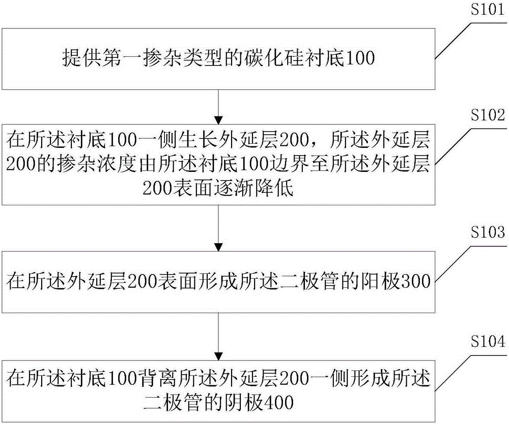
[0048] Correspondingly, the embodiment of the present invention also provides a method for manufacturing a silicon carbide Schottky diode, including:

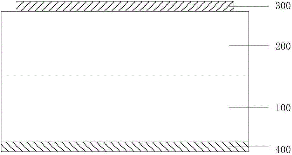
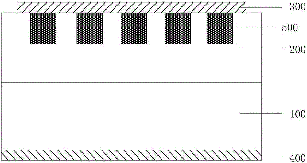
[0049] providing a silicon carbide substrate of a first doping type;

[0050] growing an epitaxial layer on one side of the substrate, the doping concentration of the epitaxial layer gradually decreases from the boundary of the substrate to the surface of the epitaxial layer;

[0051] forming an anode of the diode on the surface of the epitaxial layer;

[0052] The cathode of the diode is formed on the side of the substrate away from the epitaxial layer.

[0053] An embodiment of the present invention provides a silicon carbide Schottky diode and a manufacturing method thereof, wherein the doping concentration of the epitaxial layer of the diode gradually increases from the boundary of the anode to the boundary of the substrate. For the epitaxial layer of the diode, a high doping concentration is beneficial to reduce the on-r...


PUM


Abstract

The application discloses a silicon carbide schottky diode (SBD) and a preparation method thereof. The SBD comprises a first doped silicon carbide substrate; a cathode located on one side of the substrate; an epitaxial layer located on the side of the substrate distant from the cathode; and an anode located on the surface of the epitaxial layer, wherein the doping concentration of the epitaxial layer gradually increases from an anode boundary to a substrate boundary. For the epitaxial layer, a high concentration is in favor of reducing diode conduction resistance, and a low doping concentration is in favor of improving a diode voltage endurance capability. According to research, when a diode is in a reverse-bias state, the intensity of a built-in electric field gradually decreases from the diode anode boundary to the substrate boundary. Accordingly, the diode can reduce forward on-resistance under the condition of not changing the voltage endurance capability, and furthermore reduce conduction voltage drop and total power consumption.

Description

technical field [0001] The invention relates to the field of semiconductor devices, in particular to a silicon carbide Schottky diode and a preparation method thereof. Background technique [0002] Schottky diodes (Schottkydiode, SBD) have the advantages of low forward voltage drop and short reverse recovery time. Silicon carbide material is the preferred material for making Schottky diodes due to its wide band gap and high saturation electron drift rate. Silicon carbide Schottky diodes have high turn-off voltage, low reverse leakage current, low switching loss, etc. characteristics, making it an ideal device for high frequency and fast switching. [0003] For silicon carbide Schottky diodes, the power consumption in the forward conduction state PF=I F *V F Contributes the most to overall power consumption. Due to the SiC Schottky diode current I F is predetermined by the way it is applied, so reducing the power dissipation of a SiC Schottky diode can only be achieved b...

Claims


Application Information

Patent Timeline
IPC IPC(8): H01L29/872H01L29/06H01L21/04
CPCH01L21/0445H01L29/06H01L29/6606H01L29/872
Inventor 李诚瞻高云斌史晶晶周正东吴煜东丁荣军
Owner ZHUZHOU CRRC TIMES SEMICON CO LTD
Why Eureka
Try Eureka