Resistive random access memory and method for improving positive and negative current difference of resistive random access memory
A resistive memory and resistive technology are applied in the field of resistive memory and improving its positive and negative current difference, which can solve problems such as misreading of stored information, and achieve the effects of broad application prospects, improved reliability, and strong practicability.
- Summary
- Abstract
- Description
- Claims
- Application Information
AI Technical Summary
Problems solved by technology
Method used
Image
Examples
Embodiment 1
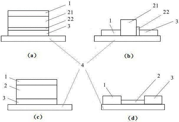
[0058] A resistive variable memory, its structure is as follows figure 1 As shown in (a), a glass substrate 4, ITO with a thickness of 200nm is used as the first terminal electrode 3, ZnO with a thickness of 15nm is used as the second resistive layer 22, and HfO with a thickness of 30nm x The first resistive switch layer 21 and Ti with a thickness of 200 nm are used as the second terminal electrode 1 .
[0059] In order to increase the positive and negative current difference of the resistive variable memory, the specific manufacturing steps are as follows:
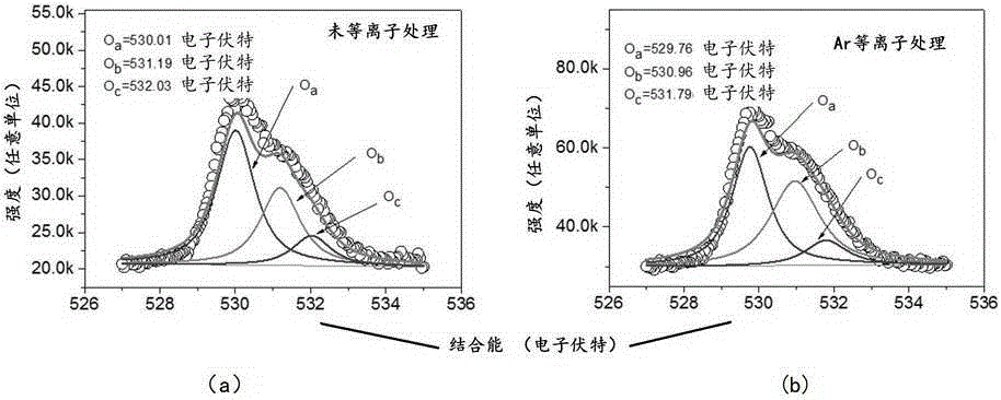
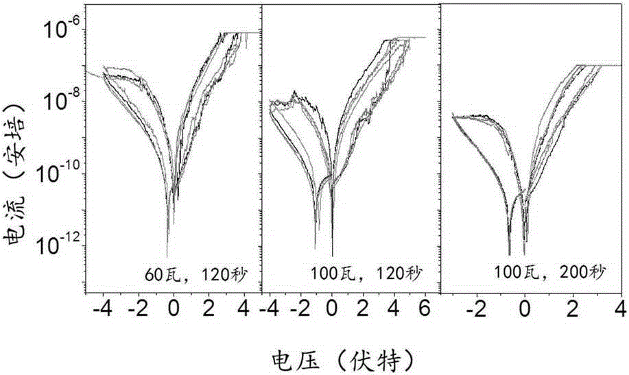
[0060] Put the glass substrate with the ITO conductive film into the vacuum chamber, and prepare 15nm ZnO as the second resistive layer 22 by magnetron sputtering; and (100 watts, 200 seconds) Ar plasma treatment of the second resistive layer 22 of ZnO with three pairs of parameters; followed by magnetron sputtering to prepare 30nm HfO x As the first resistive switch layer 21, thereby forming a double-layer storage medi...
Embodiment 2
[0063] A resistive memory whose structure is as follows figure 1 As shown in (d), the PET substrate 4, Ti with a thickness of 200 nm as the first terminal electrode 3, ZnO nanowires with a length of 10 μm and a diameter of 50 nm as the resistive medium layer 2, and Ti with a thickness of 200 nm as the first terminal electrode 3. Two terminal electrodes 1 are formed.
[0064] In order to improve the positive and negative current difference of the resistive memory, the specific manufacturing steps are as follows:
[0065] The ZnO nanowires were sprinkled on the PET substrate, and then the first terminal electrode was fabricated on the ZnO nanowires by magnetron sputtering, and then the ZnO nanowires were treated with 100 watt Ar plasma for 120 seconds, and then the ZnO nanowires were deposited on the ZnO nanowires. The second end electrode is prepared by magnetron sputtering at the other end.
[0066] It can be seen from the test, such as Figure 4 As shown, the difference be...
PUM
| Property | Measurement | Unit |
|---|---|---|
| Thickness | aaaaa | aaaaa |
| Thickness | aaaaa | aaaaa |
| Thickness | aaaaa | aaaaa |
Abstract
Description
Claims
Application Information


