Interconnection manufacturing method for film through holes in substrate

A manufacturing method and a substrate technology, which are applied in semiconductor/solid-state device manufacturing, electrical components, circuits, etc., can solve the problems of inability to realize on-line through-hole on-off detection, high contact resistance, and low reliability, and achieve reliable wiring quality, Improved wiring density and high reliability

Active Publication Date: 2016-01-13
SHANGHAI SPACEFLIGHT ELECTRONICS & COMM EQUIP RES INST
View PDF14 Cites 11 Cited by
  • Summary
  • Abstract
  • Description
  • Claims
  • Application Information

AI Technical Summary

Problems solved by technology

[0006] The object to be solved by the present invention is to provide a manufacturing method for thin film through-hole interconnection on a substrate, which overcomes the complex process, high contact resistance, low reliability, and inability to realize online through-hole on-off detection in the existing thin-film through-hole interconnection technology. question

Method used


Image

  • Interconnection manufacturing method for film through holes in substrate
  • Interconnection manufacturing method for film through holes in substrate
  • Interconnection manufacturing method for film through holes in substrate

Examples


Embodiment Construction

[0063] In order to make the above objects, features and advantages of the present invention more comprehensible, specific implementations of the present invention will be described in detail below in conjunction with the accompanying drawings.

[0064] In the following description, numerous specific details are set forth in order to provide a thorough understanding of the present invention. However, the present invention can be implemented in many other ways different from those described here, and those skilled in the art can make similar extensions without violating the connotation of the present invention, so the present invention is not limited by the specific implementations disclosed below.

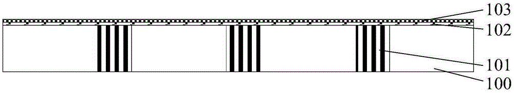
[0065] figure 1 It shows a method for fabricating thin-film through-hole interconnection on a substrate of the present invention, including the following steps:

[0066] (a1) Provide a substrate with a plurality of through holes, grind and polish the upper surface of the substrate,...


PUM

PropertyMeasurementUnit
surface roughnessaaaaaaaaaa
thicknessaaaaaaaaaa
thicknessaaaaaaaaaa

Abstract

The invention provides an interconnection manufacturing method for film through holes in a substrate. A composite adhesive layer is sputtered on the upper surface of the clean substrate; photoetching is carried out on the composite adhesive layer to form a film conduction band photoetching graph; a composite metal layer is electroplated, and a Cu layer is electroplated on the surface; removing of photoresist is carried out; photoetching is carried out at a corresponding through hole column above the Cu layer, and a film through hole photoetching graph is formed; wet etching is carried out, and the Cu layer exposed on the surface and the composite adhesive layer are removed; removing of photoresist is carried out; spin coating of benzocyclobutene (BCB) is carried out, development processing is carried out, and a dielectric film through hole graph is formed through photoetching; an ultrasonic development method is used, and development residues are removed; wet etching is carried out, the exposed Cu layer at the corresponding film through hole is removed, and the substrate is monitored online until the composite metal layer is exposed in all film through holes; the BCB dielectric layer is cured, and interconnection of film through holes in the substrate is completed. Problems that the process in the prior art is complicated, the contact resistance is large, reliability is low, through hole connection and disconnection detection can not be realized online, and the like are overcome, and interconnection of high-density through holes of multi-layer wiring of the film can be realized.

Description

technical field [0001] The invention belongs to the field of microelectronic packaging, and in particular relates to a high-density thin-film through-hole interconnection manufacturing method based on an LTCC (low temperature co-fired ceramic) substrate. Background technique [0002] With the continuous development of electronic systems in the direction of high frequency, high speed, multi-function, and miniaturization, especially the rapid development of high integration of semiconductor chips and dense input and output ports, if the substrate carrying the chip cannot achieve high-density interconnection , will become the bottleneck of the overall performance of the system. Thin-film multilayer wiring on the substrate has the advantages of high interconnection density, small signal transmission delay, and high integration, which can significantly improve the overall performance of the system, and is widely used in large-scale high-speed computer systems and digital communic...

Claims


Application Information

Patent Timeline
Patent Type & Authority Applications(China)
IPC IPC(8): H01L21/768
CPCH01L21/76816
Inventor 丁蕾陈靖杨旭一谢慧琴吴伟伟刘米丰王立春
Owner SHANGHAI SPACEFLIGHT ELECTRONICS & COMM EQUIP RES INST
Why Eureka
Try Eureka