Method for preparing graphene through plasma-enhanced chemical vapor deposition
A plasma and enhanced chemical technology, applied in gaseous chemical plating, metal material coating process, coating and other directions, to achieve the effect of low reaction temperature, convenient operation and wide source
- Summary
- Abstract
- Description
- Claims
- Application Information
AI Technical Summary
Problems solved by technology
Method used
Image
Examples
Embodiment 1
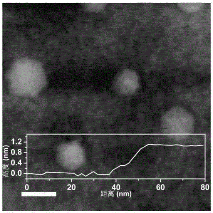
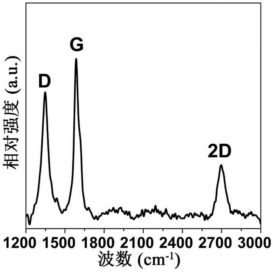
[0034] Embodiment 1, prepare graphene single crystal on the surface of silicon dioxide / silicon substrate
[0035] In the first step, the silicon dioxide / silicon substrate is ultrasonically cleaned with ethanol, acetone, and ionized water in sequence, and then dried;
[0036] In the second step, the substrate cleaned in the first step is placed in the middle of a clean quartz tube, and then the quartz tube is placed in a double-temperature zone electric furnace, so that the substrate in the quartz tube and the activated solid carbon are respectively located The central areas of the dual temperature zone electric furnaces are evacuated to vacuum.
[0037] The third step is to heat the temperature of the central area of the electric furnace where the solid carbon is located to 400°C, heat the temperature of the central area of the electric furnace where the substrate is located to 600°C, and pass hydrogen gas at a flow rate of 20 sccm for 20 minutes;
[0038] The fourth step...
Embodiment 2
[0041] Embodiment 2, prepare graphene film on silicon dioxide / silicon substrate surface
[0042] The preparation method is basically the same as that of Example 1, except that the substrate temperature is 650°C.
[0043] The atomic force microscope photograph of the product is as Figure 5 As shown, it can be observed that compared with Example 1, after the growth temperature increases, the density of graphene nanocrystal grains increases, and the grains contact each other and cover the entire substrate.
Embodiment 3
[0044] Embodiment 3, graphene film is prepared on the surface of alumina
[0045] The preparation method is basically the same as that of Example 1, except that the substrate is alumina, and the substrate temperature is 650°C.
[0046] The atomic force microscope photograph of the product is as Figure 6 As shown, it can be observed that the product morphology is similar to that of Example 2, and the graphene nanocrystal grains are in contact with each other and cover the entire substrate.
PUM
| Property | Measurement | Unit |
|---|---|---|
| power | aaaaa | aaaaa |
| height | aaaaa | aaaaa |
Abstract
Description
Claims
Application Information


