

Testing apparatus, testing method and testing circuit for semiconductor chip
A test device and test circuit technology, which is applied in the field of test devices for reverse recovery characteristics, can solve the problems of large power loss at the contact part, reduce FWD inductance, and large contact resistance, and achieve the effect of inhibiting damage
- Summary
- Abstract
- Description
- Claims
- Application Information
AI Technical Summary
Problems solved by technology
Method used
Image

Examples
Embodiment 1
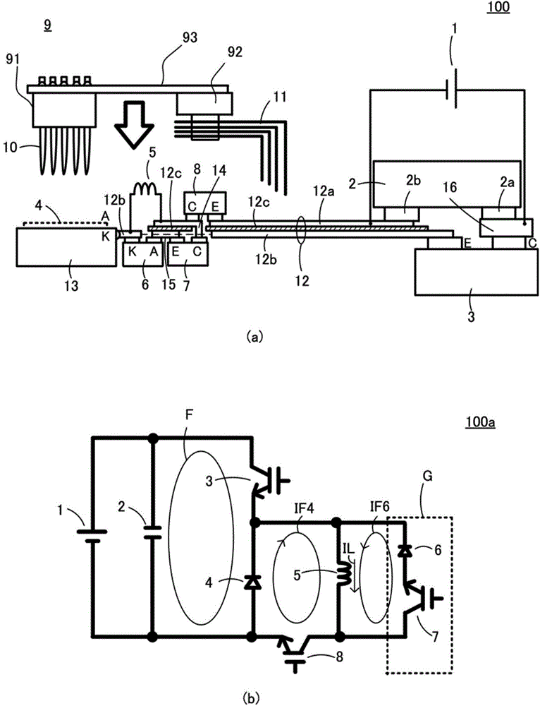
[0057] figure 1 It is a configuration diagram of main parts of the semiconductor chip testing device 100 according to the first embodiment of the present invention. This test device 100 is a test device for testing the reverse recovery characteristics of the FWD chip 4 , and can achieve low inductance of the main circuit wiring F of the test circuit 100 a and prevent damage to the test electrodes 13 .
[0058] This test device 100 includes a test electrode 13 on which the FWD chip 4 is placed, a contact probe 10 that presses the FWD chip 4 to cause a current to flow, a contact 11 , and a contact module 9 . The contacts 11 are composed of needle-shaped conductive members, and a plurality of them are arranged. The test electrode 13 is detachably provided so as to be detachable when damaged. The attachment and detachment point is the connection point between the test electrode 13 and the lower flat plate 12b. In addition, the parallel plate substrate 12 constituting the main ...
Embodiment 2
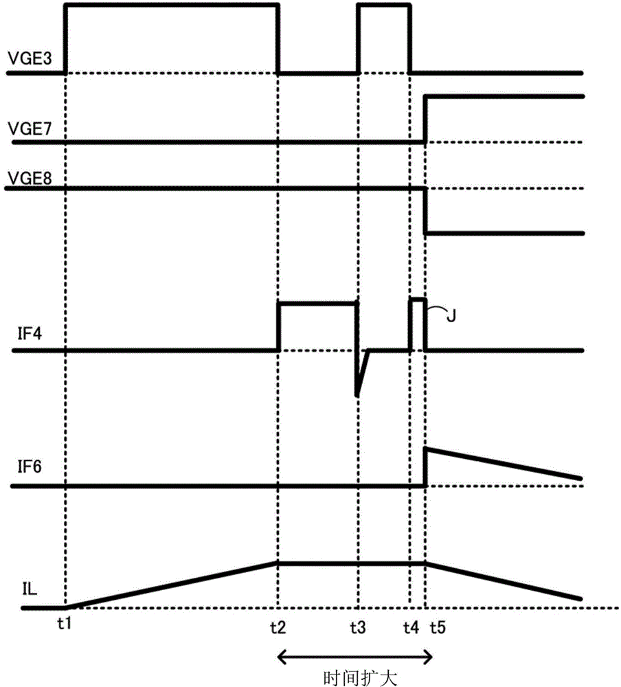
[0066] Figure 3 to Figure 10 It is an explanatory diagram explaining the test method of the second embodiment of the present invention. (a) is a cross-sectional view of the test device, and (b) is a test circuit diagram.
[0067] First, in image 3 ,exist figure 1 The FWD chip 4 is mounted on the shown test electrode 13 .
[0068] Then, in Figure 4 , the contact probe 10 is brought into contact with the anode A of the FWD chip 4 , and the cathode K of the FWD chip 4 is brought into pressure contact with the test electrode 13 . In addition, the contact 11 is brought into contact with the flat plate 12 a on the upper side of the parallel flat substrate 12 . Set IGBT8 to on state and IGBT3 to off state.
[0069] Then, in Figure 5 , the IGBT3 is turned on, and the current Io (for example, 100A) flows through the load coil 5 and the IGBT8.
[0070] Then, in Image 6 , IGBT3 is disconnected, so that the current returned to power supply 1 via the load coil and IGBT8 is d...
Embodiment 3
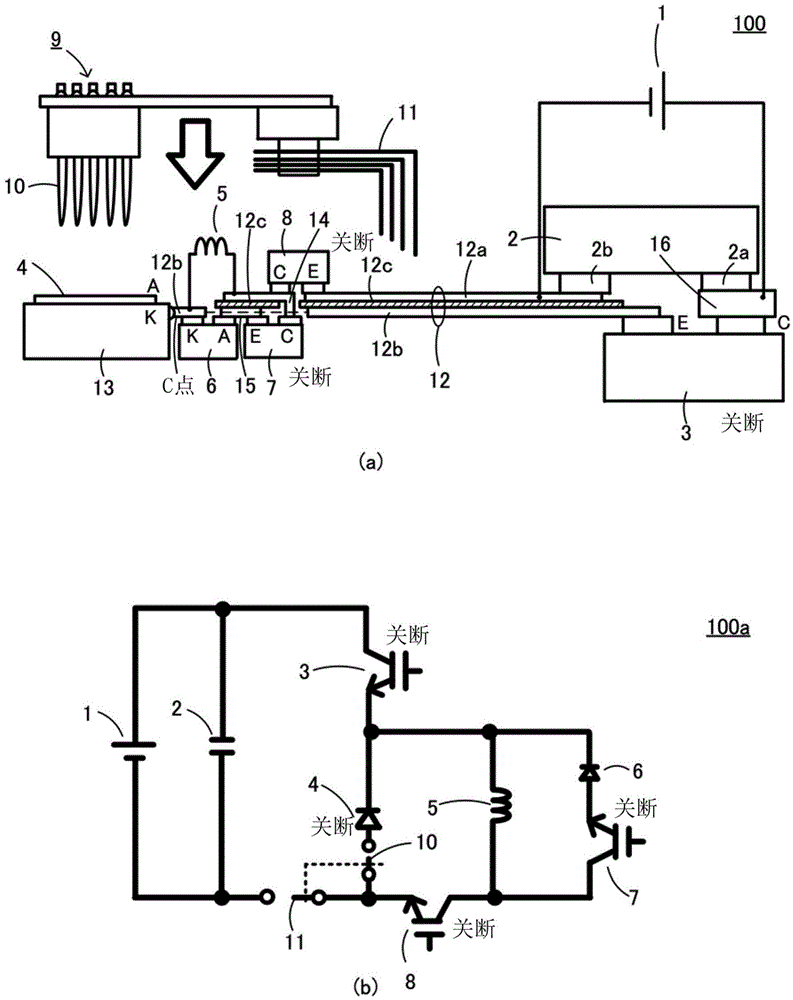
[0077] Figure 11 It is explanatory drawing of the test apparatus 200 of the semiconductor chip of the 3rd embodiment of this invention, (a) is the main part structure diagram of the test apparatus 200, (b) is the circuit diagram 200a of the test apparatus 200. and figure 1 The difference of the test device 100 is that the detour circuit G is deleted, and the resistor R is connected in parallel to the IGBT8. The reflux current IF4 flowing through FWD4 is rapidly reduced by the resistance R, thereby preventing damage to the test electrode 13 . Since there is no detour circuit G, the circuit is simplified, and the drive circuit (not shown) is also simplified.
[0078] Figure 12 It is a waveform diagram of each part. The attenuation of the reflux current IF4 in the Q portion is increased by the resistance R, and damage to the test electrode 13 can be prevented.
[0079] In addition, although the example which used IGBT as a switching element for a test was shown in the sai...
PUM
 Abstract
Description
Claims
Application Information