

A dual-wavelength single-exposure interferometry method and system
An interferometric, dual-wavelength technology, applied in the direction of measuring devices, optical devices, instruments, etc., can solve the problems of complex and time-consuming measurement process, high requirements for environmental stability, and low precision, so as to increase the measurement range, reduce the acquisition time, Effect of maintaining measurement accuracy
- Summary
- Abstract
- Description
- Claims
- Application Information
AI Technical Summary
Problems solved by technology
Method used
Image

Examples
no. 1 example
[0034] This embodiment will further illustrate the single-exposure dual-wavelength interferometry system based on the spatial carrier frequency phase shift technology described in the present invention with reference to the drawings and embodiments, but this should not limit the protection scope of the present invention.
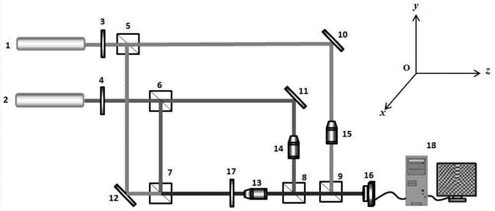
[0035] Such as figure 1 As shown, the system includes: a semiconductor-pumped solid-state laser 1 with a wavelength of 532nm and a He-Ne laser 2 with a wavelength of 632.8nm; after the two laser beams pass through the beam splitter 5 and the beam splitter 6 respectively, each Split into two beams of light, one beam of reference light and one beam of object light. After the adjustment of the plane reflector 12 and the beam splitter 7, the object light at the two wavelengths propagates in the same path, and then passes through the measured sample 17 and the reference light of the two wavelengths reflected by the plane reflectors 10 and 11 respectively. Interf...
no. 2 example
[0037] This embodiment will further illustrate the single-exposure dual-wavelength interferometry method based on the spatial carrier frequency phase shift technology described in the present invention with reference to the drawings and embodiments, but this should not limit the protection scope of the present invention.
[0038] Step 1. Collect the dual-wavelength aliasing off-axis interferogram including the spatial carrier frequency:
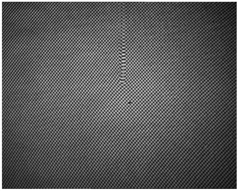
[0039] After the optical path system is built, use a computer to drive a monochrome black-and-white image sensor to collect a dual-wavelength aliasing off-axis interferogram, as shown in image 3 As shown, the interference signal intensity carrying linear carrier frequency information on the pixel point (x, y) can be expressed as:
[0040]
[0041] Among them, (x, y) represents the position of the pixel on the target surface, and the value ranges are 1≤x≤X and 1≤y≤Y respectively, and X and Y are the number of rows and columns of the dual-w...
PUM
 Abstract
Description
Claims
Application Information