Multiple-scattering super-resolution microscopic method and apparatus under micro-nano illumination

A multiple scattering and micro-nano lighting technology, applied in the field of super-resolution microscopy, can solve the problems of limited resolution, expensive, complex follow-up processing, etc., and achieve the effect of no data processing, simple device, and strong real-time performance

Active Publication Date: 2016-02-03
ZHEJIANG UNIV
View PDF4 Cites 10 Cited by
  • Summary
  • Abstract
  • Description
  • Claims
  • Application Information

AI Technical Summary

Problems solved by technology

However, the above technologies either require expensive equipment and com

Method used


Image

  • Multiple-scattering super-resolution microscopic method and apparatus under micro-nano illumination
  • Multiple-scattering super-resolution microscopic method and apparatus under micro-nano illumination
  • Multiple-scattering super-resolution microscopic method and apparatus under micro-nano illumination

Examples


Embodiment 1

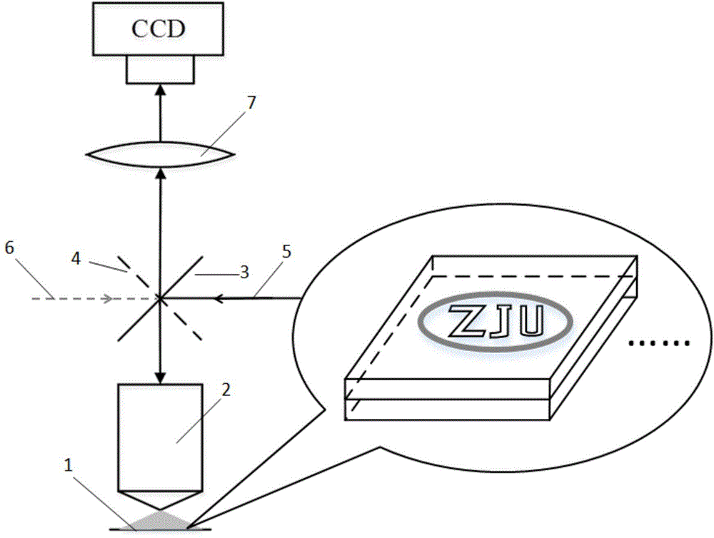
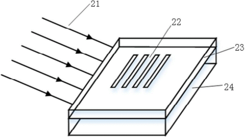
[0061] Such as figure 2 As shown, the slab waveguide is selected as the micro-nano light source in this embodiment, the sample 22 to be observed is placed on the slab waveguide with a thickness of 300 nanometers, the sample is located on the surface of the waveguide layer 23, the substrate is located at the bottom of the waveguide layer 23, and the substrate For the reflective layer 24, the light 21 with a wavelength of 500nm is coupled into the waveguide through a free optical path or an optical fiber bundle to form a micro-nano light source, and the coupled light can be in the visible or near-ultraviolet band.

[0062] In the process of waveguide surface field scattering, a magnified virtual image under the surface of the two-dimensional object will be formed. The whole device is observed under a high-power optical microscope, and the focus is adjusted to make the image clear. Use a 5 million pixel CCD to take pictures of the image, and process and restore the image in the ...

Embodiment 2

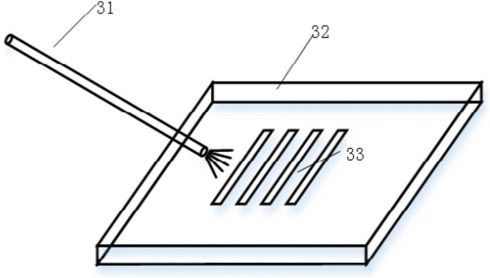
[0064] Such as image 3 As shown, a waveguide micro-nano fiber is used as the micro-nano light source in this embodiment, and the sample 33 is placed on the substrate 32 on the stage of a high-power optical microscope so that it is located near the focal plane of the objective lens. Fix the micro-nano optical fiber 31 on the precision three-dimensional translation stage, and approach it in a direction that forms an angle of 7 degrees with the horizontal plane (determined according to the height of the microscope stage and the height of the three-dimensional translation platform on which the micro-nano optical fiber is fixed, with a uniform illumination effect) sample. The laser or broadband light emitted by the external light source is coupled into the micro-nano fiber 31 . The distance between the micro-nano fiber 31 and the sample 33 is adjusted so that the target is illuminated by the light emitted by the micro-nano fiber, and the focus is adjusted slightly to make the ima...

Embodiment 3

[0068] Such as Figure 4 As shown, a combination of nanowires and a double-layer substrate is used to introduce a double optical path as the micro-nano light source in this implementation, the excitation light is coupled into the microscope illumination optical path, and the sample 43 is placed on a silicon-based silicon dioxide substrate 42 or embedded To the surface of the substrate, the bottom of the substrate is a reflective layer 44, and the thickness of the silicon dioxide layer is 300 nanometers. The substrate 42 is placed under a high-power optical microscope, so that the sample 43 is located on the focal plane of the objective lens. Using a micro-nano fiber connected to a three-dimensional precision stage (such as Figure 7 shown), perform three-dimensional micro-nano operations on the nanowire 41, place a CdS-doped nanowire with a diameter of 300 nanometers on the substrate near the sample 43, and bend the nanowire 41 according to the contour of the sample 43. The n...


PUM

PropertyMeasurementUnit
Thicknessaaaaaaaaaa
Diameteraaaaaaaaaa
Diameteraaaaaaaaaa

Abstract

The present invention discloses a multiple-scattering super-resolution microscopic method under micro-nano illumination including the steps as follows: 1) employing a micro-nano light source as a micro-nano structure sample having single spatial frequency so that the multiple scattering appears in the interior of the micro-nano structure sample; 2) performing light field imaging for the sample having single spatial frequency through a microscope, and performing spectral analysis for the imaging so as to obtain the frequency shift amount of the micro-nano light source; 3) replacing the structural sample having single spatial frequency with a structural sample having various single spatial frequencies, and establishing a frequency shift database of the micro-nano light source corresponding to various spatial frequencies; 4) observing the sample to be detected by utilizing the micro-nano light source, irradiating the sample to be detected within a 360-degree range, and performing imaging through the microscope during the irradiation process so as to obtain the corresponding frequency shift image. 5) performing frequency spectrum reduction and reconstruction for the frequency shift image according to the frequency shift database so as to obtain the super-resolution microscopic image of the sample to be detected. The present invention also discloses a multiple-scattering super-resolution microscopic apparatus under micro-nano illumination.

Description

technical field [0001] The invention relates to the field of super-resolution microscopy, in particular to a multiple scattering super-resolution microscopy method and device under micro-nano illumination. Background technique [0002] According to Abbe's diffraction limit theory, the limit resolution of conventional far-field optical microscope can be expressed as Where λ is the wavelength of the illumination light used, and NA is the numerical aperture of the microscope objective lens used. Therefore, in the visible light band, the resolution of optical microscopy is limited to around 200 nanometers. However, with the development of biomedicine and other technologies, researchers have begun to analyze biological tissues and cells at the nanoscale, and the properties of the observed samples are also diverse. A new technology that can break through the conventional diffraction limit to achieve super-resolution microscopy. [0003] Diffraction-limited resolution can also ...

Claims


Application Information

Patent Timeline
IPC IPC(8): G02B21/06G02B21/36G01N21/00
Inventor 杨青刘小威刘旭李海峰匡翠方郝翔周雅旋
Owner ZHEJIANG UNIV
Why Eureka
Try Eureka