A kind of memory and its manufacturing method
A manufacturing method and memory technology, applied in electrical components and other directions, can solve the problems of uncertain resistance value distribution of high and low resistance values of phase change memory, and achieve the effects of low power consumption, high density and large capacity
- Summary
- Abstract
- Description
- Claims
- Application Information
AI Technical Summary
Problems solved by technology
Method used
Image
Examples
Embodiment 1
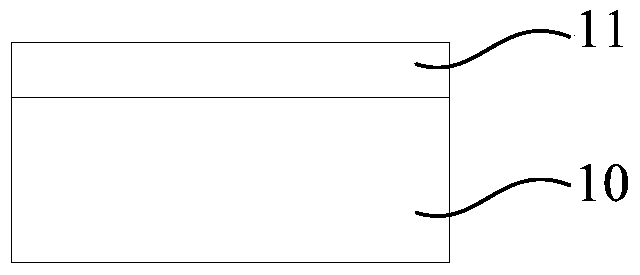
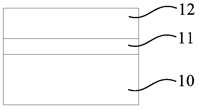
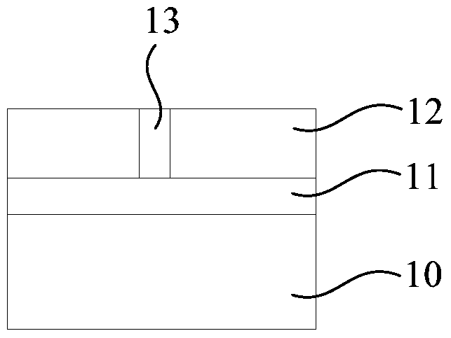
[0047] The present invention provides a memory, which at least includes: figure 1 The substrate 10 shown and the bottom electrode 11 formed on the upper surface of the substrate 10; preferably, the substrate is a semiconductor substrate, and the substrate in this embodiment is a silicon substrate; preferably, the The material of the bottom electrode 11 is a metal conductive material; as figure 2 As shown, the memory also includes a dielectric layer 12 located on the bottom electrode 11, preferably, the material of the dielectric layer 12 includes SiO 2 、SiN x 、AL 2 o 3 or ZrO 2 any of the. The material of the dielectric layer 12 in the present embodiment is SiO 2 ; Further preferably, the thickness of the dielectric layer is 100nm-300nm; as image 3 As shown, the dielectric layer 12 is provided with through holes 13, such as Figure 4 As shown, the through hole 13 is filled with metal, preferably, the diameter of the through hole is 50nm-300nm; the material of the me...
Embodiment 2
[0060] The difference between the memory in this embodiment and the memory in Embodiment 1 is that the composite storage structure is different. In this embodiment, the composite storage structure includes an oxide on the upper surface of the dielectric layer and an oxide on the The chalcogenide compound 141 on the upper surface of the oxide 142 , that is, the oxide and the chalcogenide compound in the composite storage structure in this embodiment and the oxide and the chalcogenide compound in the first embodiment are exactly upside down. In this embodiment, the two-layer stacked structure constituting the composite storage structure includes: an oxide located on the upper surface of the dielectric layer and in contact with the metal in the through hole, and a chalcogenide compound located on the upper surface of the oxide ; the oxide and the chalcogenide are in contact with each other.
[0061] Meanwhile, the method for forming the composite memory structure in this embodime...
Embodiment 3
[0065] This embodiment provides a memory, which at least includes: figure 1 The substrate 10 shown and the bottom electrode 11 formed on the upper surface of the substrate 10; preferably, the substrate is a semiconductor substrate, and the substrate in this embodiment is a silicon substrate; preferably, the The material of the bottom electrode 11 is a metal conductive material; as figure 2 As shown, the memory also includes a dielectric layer 12 located on the bottom electrode 11, preferably, the material of the dielectric layer 12 includes SiO 2 、SiN x 、AL 2 o 3 or ZrO 2 any of the. The material of the dielectric layer 12 in the present embodiment is SiO 2 ; Further preferably, the thickness of the dielectric layer is 100nm-300nm; as image 3 As shown, the dielectric layer 12 is provided with through holes 13, such as Figure 4 As shown, the through hole 13 is filled with metal, preferably, the diameter of the through hole is 50nm-300nm; the metal in the through hol...
PUM
| Property | Measurement | Unit |
|---|---|---|
| thickness | aaaaa | aaaaa |
| diameter | aaaaa | aaaaa |
| thickness | aaaaa | aaaaa |
Abstract
Description
Claims
Application Information


