
Coating method for cavity surface of semiconductor laser chip

A laser and semiconductor technology, used in semiconductor lasers, lasers, laser parts, etc., can solve the problems of poor product reliability, affecting product service life, unstable laser performance, etc., to improve service life and reliability. , The effect of moisture isolation, long-term aging performance and anti-static ESD ability improvement

Active Publication Date: 2021-11-26
湖北光安伦芯片有限公司
View PDF8 Cites 0 Cited by
  • Summary
  • Abstract
  • Description
  • Claims
  • Application Information

AI Technical Summary

Problems solved by technology

[0002] In order to improve the service life of the semiconductor laser chip and improve the reliability of the product, it is necessary to coat the front and rear cavity surfaces of the chip to protect the cavity surface and realize the reduction of the laser threshold and the power of the laser through different film characteristics of the cavity surface. Especially as the current high-speed chips generally use the InGaAlAs structure when doping, Al is easily oxidized in the air, and the cavity surface formed by cleavage is easily oxidized to form oxide defects. It is easy to form heat accumulation at the defect, which will affect the quality of the film layer on the cavity surface, increase the risk of film failure, directly lead to unstable laser performance, poor product reliability, and directly affect the service life of the product; at the same time, for For chips with Al structure, the structure of the cavity film system, the shape of the film layer, and its stable optical performance are all important factors that directly affect the laser chip, which can make the performance and reliability of the chip more stable. Stronger impact resistance, more stable light output and longer life

Method used


Image

  • Coating method for cavity surface of semiconductor laser chip
  • Coating method for cavity surface of semiconductor laser chip
  • Coating method for cavity surface of semiconductor laser chip

Examples


Embodiment 1

[0048] A method for coating a cavity surface of a semiconductor laser chip, comprising the steps of:

[0049] 1) Carry out bar strip cleavage and clip strips for the chip to be coated, and quickly put it into the evaporation coating equipment (to ensure that the product is exposed to the air as short as possible after cleavage), vacuumize, ensure a high vacuum environment, and reduce Process impurity gas, improve product surface activity;

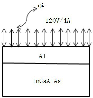
[0050] 2) Perform ion source pre-cleaning treatment on the surface of the optical cavity of the chip; the specific process is: wait for the vacuum degree in the equipment to reach 2.5×10 -6 During Torr, the Hall ion source is used to feed argon gas, the anode voltage of the ion source is controlled to 120V, the anode current is controlled to 4A, the neutralization current is controlled to 260mA, and the treatment time is 200s; using this process condition for plasma treatment, an excellent The surface cleaning effect of the cavity surface ...

Embodiment 2

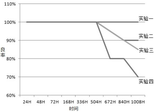
[0055] Carry out long-term aging performance test to the product of experiment, experiment is divided into four groups, and the manufacture method of four groups of experimental products is the same as embodiment 1, and difference is:

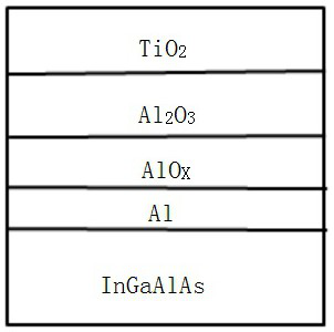
[0056] Experiment 1 is the experimental group: both the surface of the light cavity and the surface of the backlight cavity adopt the Al layer oxygen penetration process, and the film structure of the surface of the light cavity is Al / AlO X / Al 2 o 3 / TiO 2 , the film structure of the backlight cavity surface is Al / AlO X / Al 2 o 3 / Si / Al 2 o 3 / Si, randomly select 20pcs chips;

[0057] Experiment 2 is the control group: the Al layer oxygen permeation process is adopted on the surface of the light cavity, and the film structure of the surface of the light cavity is Al / AlO X / Al 2 o 3 / TiO 2 , the film structure of the backlight cavity surface is Al 2 o 3 / Si / Al 2 o 3 / Si, randomly select 20pcs chips;

[0058] Experiment 3 is the ...

Embodiment 3

[0063] The product of experiment is carried out SEM topography analysis, experiment is divided into two groups, and the preparation method of two groups of experimental products is the same as embodiment 1, and difference is:

[0064] Experiment 1 is the experimental group: both the surface of the light cavity and the surface of the backlight cavity adopt the Al layer oxygen penetration process, and the film structure of the surface of the light cavity is Al / AlO X / Al 2 o 3 / TiO 2 , the film structure of the backlight cavity surface is Al / AlO X / Al 2 o 3 / Si / Al 2 o 3 / Si, randomly select 20pcs chips;

[0065] Experiment 2 is the control group; neither the surface of the light cavity nor the surface of the backlight cavity adopts the Al layer oxygen penetration process, and the film structure of the surface of the light cavity is Al 2 o 3 / TiO 2 , the film structure of the backlight cavity surface is Al 2 o 3 / Si / Al 2 o 3 / Si, randomly select 20pcs chips;

[0066...


PUM

PropertyMeasurementUnit
thicknessaaaaaaaaaa

Abstract

The invention belongs to the technical field of semiconductor laser end surface coating, and particularly relates to a coating method for a cavity surface of a semiconductor laser chip. The coating method comprises the following steps of 1) performing Bar strip cleavage and strip clamping on a chip to be coated, quickly putting the chip into evaporation coating equipment, and vacuumizing; 2) carrying out ion source pre-cleaning treatment on the light emitting cavity surface of the chip; 3) plating a high anti-reflection film system on the light emitting cavity surface of the chip, wherein the high anti-reflection film system at least comprises a first Al layer and a first AlOX layer; firstly plating an Al layer, and then introducing O2 by using an ion source to carry out oxidation treatment; 4) carrying out ion source pre-cleaning treatment on the backlight cavity surface of the chip; and 5) plating a high-reflective film system on the backlight cavity surface of the chip, the high-reflective film system at least comprising a second Al layer and a second AlOX layer, firstly plating the Al layers, and then introducing O2 by using an ion source for oxidation treatment. According to the method, the Al layers are plated on the front cavity surface and the rear cavity surface of the chip, and partial oxidation is performed, so that the effect of protecting the laser semiconductor cavity surface is achieved, and the reliability problem caused by oxidation of the cavity surface is further avoided.

Description

technical field [0001] The invention belongs to the technical field of film coating on the end face of a semiconductor laser, and in particular relates to a film coating method for a cavity face of a semiconductor laser chip. Background technique [0002] In order to improve the service life of the semiconductor laser chip and improve the reliability of the product, it is necessary to coat the front and rear cavity surfaces of the chip to protect the cavity surface and realize the reduction of the laser threshold and the power of the laser through different film characteristics of the cavity surface. Especially as the current high-speed chips generally adopt the InGaAlAs structure when doping, Al is easily oxidized in the air, and the cavity surface formed by cleavage is easily oxidized to form oxide defects, resulting in It is easy to form heat accumulation at the defect, which will affect the quality of the film layer on the cavity surface, increase the risk of film failur...

Claims


Application Information

Patent Timeline
Patent Type & Authority Applications(China)
IPC IPC(8): C23C14/24C23C14/18C23C14/08C23C14/02C23C8/12C23C14/58H01S5/028
CPCC23C14/24C23C14/18C23C14/022C23C14/081C23C14/5853C23C8/12C23C14/083H01S5/0283Y02P70/50
Inventor 赵军游顺青陈锋
Owner 湖北光安伦芯片有限公司
Learn More