Low-leakage high-reliability low-voltage transient suppression diode chip and production method

A technology of transient suppression and production method, applied in the direction of circuits, electrical components, semiconductor devices, etc., can solve problems such as unstable breakdown voltage, poor product reliability, large reverse breakdown leakage, etc., to avoid local current Excessive, prolong life, reduce the effect of reverse leakage current

Active Publication Date: 2019-01-18
上海瞬雷科技有限公司
View PDF3 Cites 0 Cited by
  • Summary
  • Abstract
  • Description
  • Claims
  • Application Information

AI Technical Summary

Problems solved by technology

There are problems in the existing technology: when a single diffusion junction is used in the production of transient suppression diode chips, the surface breakdown voltage of the mesa is lower than the internal breakdown voltage during reverse breakdown, causing the surface breakdown to precede the internal breakdown, and the breakdown current Concentrated distribution near the countertop, the countertop is composed of silicon and glass layers, the stress between them is relatively large, resulting in large reverse breakdown leakage, so products with reverse breakdown voltage of low-voltage transient suppression diodes in the industry less than 10V have reverse leakage Larger, generally 500-1000μA, and due to increased leakage, the junction temperature rises and the product reliability deteriorates.
At the same time, the junction depth of paper source diffusion is not flat, resulting in unstable breakdown voltage and poor surge resistance

Method used


Image

  • Low-leakage high-reliability low-voltage transient suppression diode chip and production method
  • Low-leakage high-reliability low-voltage transient suppression diode chip and production method
  • Low-leakage high-reliability low-voltage transient suppression diode chip and production method

Examples


Embodiment 1

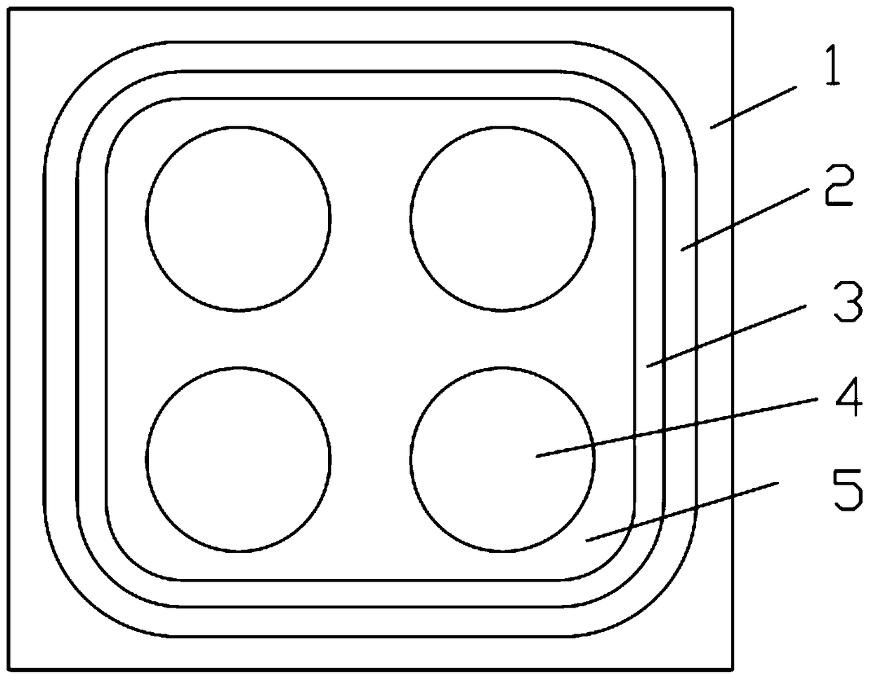
[0063] In this embodiment, the unidirectional low-leakage high-reliability low-voltage transient suppression diode chip production method provided by the present invention, such as figure 1 As shown, the front structure of the unidirectional / bidirectional low-leakage high-reliability low-voltage transient suppression diode chip is as follows: chip 1; corrosion mesa 2; glass edge 3; P + diffusion junction 4; metal layer 5.

[0064] Such as Figure 4 As shown, the cross-sectional structure of the unidirectional low-leakage high-reliability low-voltage transient suppression diode chip is as follows: chip 1; glass edge 2; P+ diffusion junction 4; metal layer 5; N+ diffusion junction 6; P ++ Diffusion junction7.

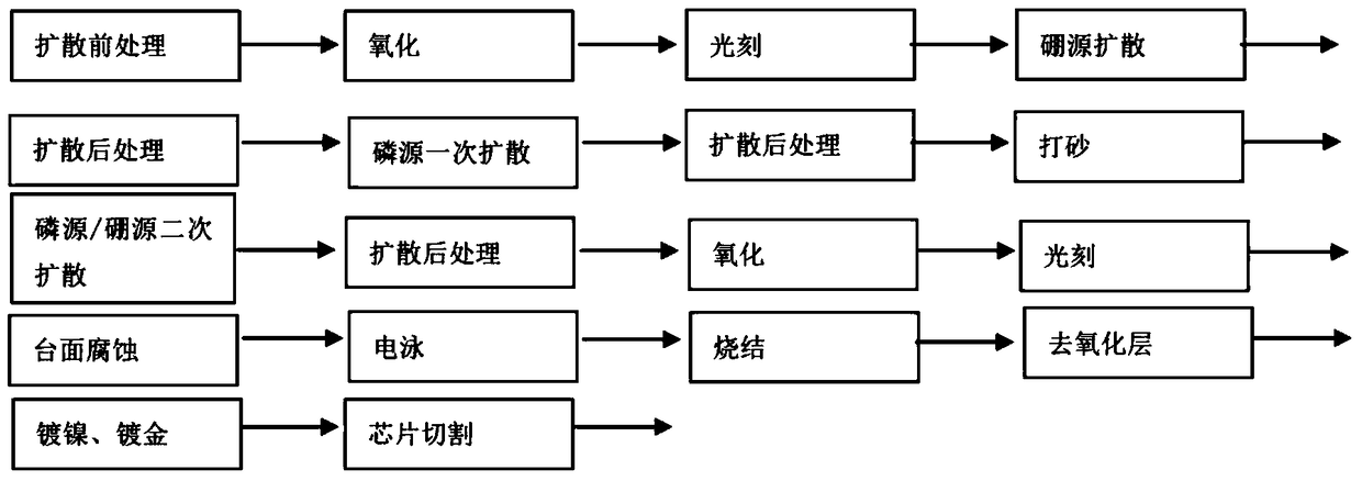
[0065] Such as figure 2 As shown, the production method of the unidirectional low-leakage high-reliability low-voltage transient suppression diode chip provided by the present invention, the flow process is as follows:

[0066] Step 1: Pre-diffusion treatment: chemic...

Embodiment 2

[0087] Such as Figure 5 As shown, in this embodiment, the bidirectional low-leakage high-reliability low-voltage transient suppression diode chip cross-sectional structure provided by the present invention is as follows: chip 1; glass edge 3; P + Diffusion junction 4; metal layer 5; N + Diffusion junction6.

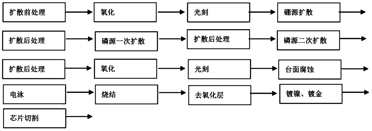
[0088] The bidirectional low-leakage high-reliability low-voltage transient suppression diode chip production method provided by the present invention comprises the following steps:

[0089] Step 1: Diffusion pre-treatment, through acid, alkali, deionized water ultrasonic cleaning and other processes, chemically treat the surface of the silicon wafer to make the surface of the silicon wafer unstained;

[0090] Step 2: For the first oxidation, put the silicon wafer that has been pre-diffused in an oxidation furnace at 1100-1200°C to grow a first oxide layer; the thickness of the first oxide layer is

[0091] Step 3: For the first photolithography, the oxidized silico...


PUM


Abstract

The invention provides a low-voltage transient-suppression diode chip with low electric leakage and high reliability and a production method, comprising one-way and two-way structures and a production method. Specifically, a plurality of independent P+ diffused junctions are additionally arranged at the lower part of an N+ diffused junction, so that puncturing is firstly carried out in a chip body during chip puncturing, surface puncturing is avoided, and electric leakage is reduced; and moreover, the voltage uniformity can be higher, reverse surge capacity stability and reliability of a diode are guaranteed, and the service life of the diode is prolonged. The technologies of gas source diffusion technology, low-temperature groove corrosion, glass powder double-faced one-time electrophoresis and the like, and the structure and production technology of the new transient-suppression diode chip are designed, so that puncturing is firstly carried out in the chip body during chip puncturing, surface puncturing is avoided, and the voltage uniformity can be higher.

Description

technical field [0001] The invention relates to the production technology of a crystal diode chip, in particular to a low-voltage transient suppression diode chip with low leakage and high reliability and a production method. Background technique [0002] At present, the production of low-voltage transient suppression diode (TVS) chips in the semiconductor industry usually adopts the production process of twice-diffusion of a single junction from a paper source. There are problems in the existing technology: when a single diffusion junction is used in the production of transient suppression diode chips, the surface breakdown voltage of the mesa is lower than the internal breakdown voltage during reverse breakdown, causing the surface breakdown to precede the internal breakdown, and the breakdown current Concentrated distribution near the countertop, the countertop is composed of silicon and glass layers, the stress between them is relatively large, resulting in large reverse...

Claims


Application Information

Patent Timeline
Patent Type & Authority Patents(China)
IPC IPC(8): H01L29/66H01L29/861
CPCH01L29/66136H01L29/8613
Inventor 盛锋
Owner 上海瞬雷科技有限公司
Why Eureka
Try Eureka