LED chip and manufacturing method thereof

An LED chip and electrode technology, applied in electrical components, circuits, semiconductor devices, etc., can solve problems such as uneven current distribution of LED chips, and achieve the effects of improving luminous performance, enhancing lateral flow, and improving uniformity.

Inactive Publication Date: 2016-03-02
HUIZHOU BYD IND
View PDF6 Cites 5 Cited by
  • Summary
  • Abstract
  • Description
  • Claims
  • Application Information

AI Technical Summary

Problems solved by technology

[0004] In order to improve the defect of uneven current distribution of existing LED chips, the present invention provides an LED chip and a manufacturing method thereof, which can enhance the lateral flow of LED chip current, improve the uniformity of current distribution, and improve the luminous performance of the LED chip

Method used


Image

  • LED chip and manufacturing method thereof
  • LED chip and manufacturing method thereof
  • LED chip and manufacturing method thereof

Examples


Embodiment Construction

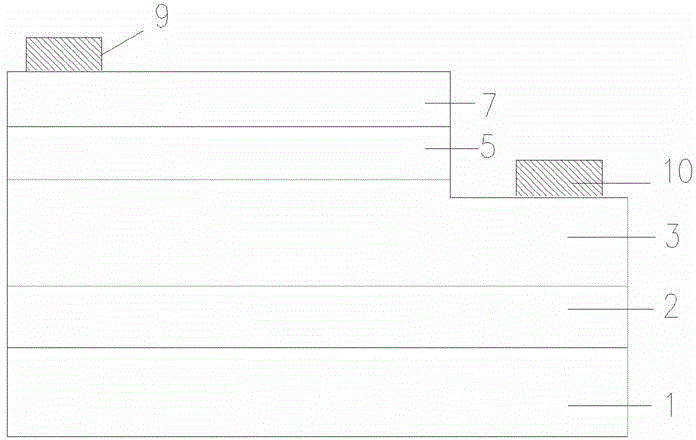
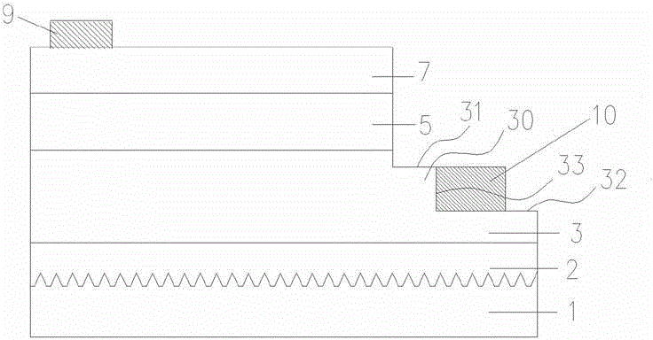
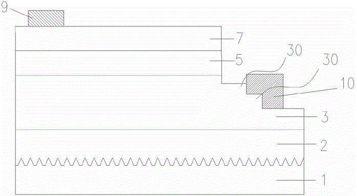
[0012] In order to make the technical problems, technical solutions and beneficial effects solved by the present invention clearer, the present invention will be further described in detail below in conjunction with the embodiments. It should be understood that the specific embodiments described here are only used to explain the present invention, not to limit the present invention.

[0013] In describing the present invention, it should be understood that the terms "center", "longitudinal", "transverse", "length", "width", "thickness", "upper", "lower", "front", " Orientation or position indicated by "back", "left", "right", "vertical", "horizontal", "top", "bottom", "inner", "outer", "clockwise", "counterclockwise", etc. The relationship is based on the orientation or positional relationship shown in the drawings, and is only for the convenience of describing the present invention and simplifying the description, rather than indicating or implying that the referred device or...


PUM


Abstract

The invention provides an LED chip comprising a substrate, a buffer layer, an N-type semiconductor layer, a light-emitting layer that partially covers the N-type semiconductor layer, a P-type semiconductor layer and a conductive layer, wherein the above layers are formed on the substrate in turn. The region of the N-type semiconductor layer, which is not covered by the light-emitting layer, serves as an N electrode mounting region. The N electrode mounting region is provided with a step and the step is composed of a first step surface, a second step lower than the first step surface, and a step side surface positioned between the first step surface and the second step surface. The LED chip further comprises a P electrode and an N electrode. The P electrode is formed on the conductive layer. The N electrode is formed on the second step surface and is in contact with the step side surface. The N electrode mounting region of the LED chip is provided with the step structure, and an N electrode is formed on the step structure. Compared with a conventional LED chip with electrodes formed on the same side thereof, the N electrode is in contact with the sidewall of the N-type semiconductor layer, so that the current lateral flow is enhanced. The current distribution uniformity is improved. Meanwhile, the light emitting performance of the LED chip is effectively improved.

Description

technical field [0001] The invention belongs to the field of semiconductors, in particular to an LED chip and a manufacturing method. Background technique [0002] Light-emitting diode (LED) is a junction-type electroluminescent semiconductor device that can convert electrical signals into light signals. Gallium nitride-based light-emitting diodes, as solid-state light sources, are known for their high efficiency, long life, energy saving and environmental protection, and small size. Such advantages have become the focus of research and development and industry in the international semiconductor and lighting fields, and are mainly based on gallium nitride (GaN), indium gallium nitride (InGaN), aluminum gallium nitride (AlGaN) and indium aluminum gallium nitride (AlGaInN) The Group III-V nitride material has a continuously adjustable direct bandwidth of 0.7-6.2eV, covering the spectral range from ultraviolet light to infrared light, and is an ideal material for manufacturing ...

Claims


Application Information

Patent Timeline
Patent Type & Authority Applications(China)
IPC IPC(8): H01L33/02H01L33/00
Inventor 谢春林
Owner HUIZHOU BYD IND
Why Eureka
Try Eureka