Preparation method of TFT array substrate, array substrate and display device

A technology for array substrates and pattern layers, which is applied in semiconductor/solid-state device manufacturing, optics, instruments, etc., can solve the problems of large number of masks and increased costs, and achieve the effect of reducing costs

Active Publication Date: 2016-03-09
SHENZHEN CHINA STAR OPTOELECTRONICS TECH CO LTD
View PDF3 Cites 11 Cited by
  • Summary
  • Abstract
  • Description
  • Claims
  • Application Information

AI Technical Summary

Problems solved by technology

[0005] The present invention provides a method for preparing a TFT array substrate, an array substrate and a display device, which can solve the problem in the prior art that the cost is increased due to the large number of required photomasks

Method used


Image

  • Preparation method of TFT array substrate, array substrate and display device
  • Preparation method of TFT array substrate, array substrate and display device
  • Preparation method of TFT array substrate, array substrate and display device

Examples


Embodiment Construction

[0028] The present invention will be described in detail below in conjunction with the accompanying drawings and specific embodiments.

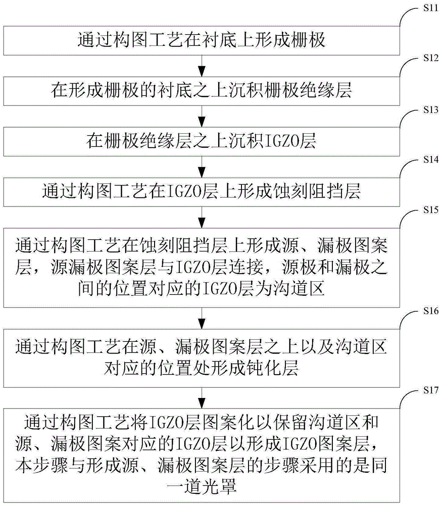
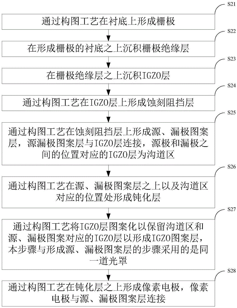
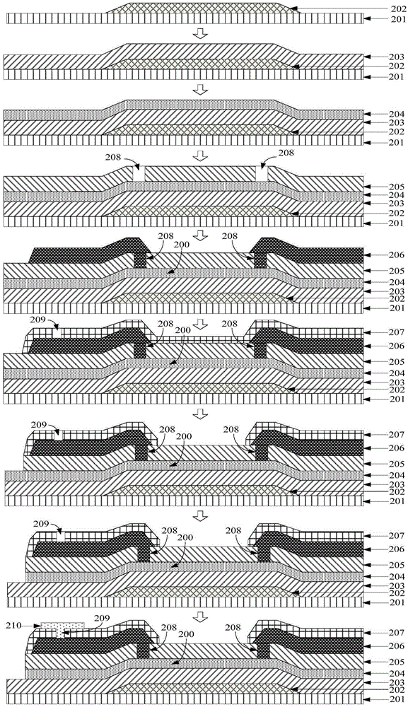
[0029] see figure 1 , figure 1 It is a schematic flow chart of the first embodiment of the manufacturing method of the TFT array substrate of the present invention.

[0030] S11, forming a gate on the substrate through a patterning process.

[0031] The gate is formed of metal, such as molybdenum, copper, aluminum and aluminum alloy, or a metal compound conductive layer formed by stacking aluminum layer, tungsten layer and chromium layer.

[0032] S12 , depositing a gate insulating layer on the substrate for forming the gate.

[0033] The gate insulating layer is formed by CVD or PECVD technology. The gate insulating layer can be one layer or two layers. One layer can be SiO 2 、SiN x Or AlO, the second layer generally uses SiN x .

[0034] S13, depositing an IGZO layer on the gate insulating layer.

[0035] The IGZO layer is used as t...


PUM


Abstract

The invention provides a preparation method of a TFT array substrate, the array substrate and a display device. The preparation method comprises that a grid is formed on a substrate by a composition technology; a grid insulating layer is deposited on the substrate which forms the grid; an IGZO layer is deposited on the grid insulating layer; an etching barrier layer is formed on the IGZO layer by the composition technology; a source and drain pattern layer is formed on the etching barrier layer via the composition technology, and connected with the IGZO layer, and the part, corresponding to position between source and drain electrodes, of the IGZO layer serves as a channel region; a passivation layer is formed on the source and drain pattern layer at the position corresponding to the channel region; and the IGZO layer is patterned by the composition technology to keep the channel region and the part, corresponding to the source and drain pattern layer, of the IGZO layer to form an IGZO pattern layer, and a photomask used in the step of forming the IGZO pattern layer is the same with that used in the step of forming the source and drain pattern layer. One photomask can be saved, and thus, the production cost is reduced.

Description

technical field [0001] The invention relates to the technical field of liquid crystal display, in particular to a preparation method of a TFT array substrate, an array substrate and a display device. Background technique [0002] Thin Film Transistor Liquid Crystal Display (TFT-LCD for short) has the characteristics of small size, low power consumption, and no radiation, and has been developed rapidly in recent years. In the liquid crystal panel industry, with the current large-scale display industry, the demand for high resolution is becoming stronger and stronger, and higher requirements are put forward for the charging and discharging of active layer semiconductor devices. [0003] IGZO (indium gallium zinc oxide, indium gallium zinc oxide) is an amorphous oxide containing indium, gallium, and zinc. It has high mobility, and the carrier mobility is 20 to 30 times that of amorphous silicon, which can greatly improve the TFT. The charge and discharge rate of the pixel elec...

Claims


Application Information

Patent Timeline
Patent Type & Authority Applications(China)
IPC IPC(8): H01L27/12H01L21/77G02F1/1333
CPCG02F1/1333H01L21/77H01L27/1214H01L27/1288
Inventor 周志超
Owner SHENZHEN CHINA STAR OPTOELECTRONICS TECH CO LTD
Why Eureka
Try Eureka