
Single crystal silicon growth control method

A technology of growth control and monocrystalline silicon, which is applied in the direction of single crystal growth, single crystal growth, crystal growth, etc., can solve the problems of reducing production efficiency, exacerbating crystal temperature gradient, and reducing the length of silicon single crystal rods, etc.

Active Publication Date: 2019-05-07
SHANGHAI ADVANCED SILICON TECH CO LTD
View PDF7 Cites 1 Cited by
  • Summary
  • Abstract
  • Description
  • Claims
  • Application Information

AI Technical Summary

Problems solved by technology

There are two basic ways to achieve it, one is to reduce the length of the silicon single crystal rod, but it will greatly reduce the production efficiency
The second is to lower the temperature of the silicon single crystal rod, but the method of cooling may aggravate the temperature gradient in the radial direction of the crystal, which will be transferred to the growth interface, resulting in a decrease in the quality of the supercrystal

Method used


Image

  • Single crystal silicon growth control method
  • Single crystal silicon growth control method

Examples


Embodiment 1

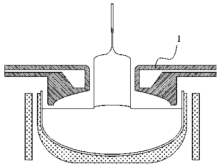
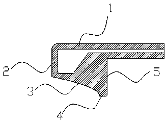
[0021] The long diameter is an 8-inch monocrystalline silicon rod, and the inner diameter is a 22-inch (560mm inner diameter) quartz crucible. The height of the erected surface 2 in the reflection and cooling device is 250 mm, and the surface roughness is controlled at 8-10 μm by shot blasting. The silicon carbide porous ceramic coating is plated on the surface by the plasma vapor deposition method, the thickness of the coating is 2.42 μm, the inner pore size of the coating is controlled at 1.2 μm-1.5 μm, and the density is greater than 65%. The first vertical section (2) is 20mm away from the side surface of the single crystal silicon rod.

[0022] The semi-parabolic arc section (3), the opening of the parabola faces the ingot, the opening height is 130mm, and the length of the arc section (3) is 130mm. Horizontal section (4) length is 20mm. The distance between the second vertical section (5) and the crucible wall is 10mm. The semi-parabolic arc section (3), the horizonta...

Embodiment 2

[0027] The long diameter is an 8-inch single crystal silicon rod, and the inner diameter is a 24-inch (610mm inner diameter) quartz crucible. The height of the erected surface 2 in the reflection and cooling device is 250 mm, and the surface roughness is controlled at 8-10 μm by shot blasting. The silicon carbide porous ceramic coating is plated on the surface by the plasma vapor deposition method, the thickness of the coating is 2.42 μm, the inner pore size of the coating is controlled at 1.2 μm-1.5 μm, and the density is greater than 65%. The first vertical section (2) is 20mm away from the side surface of the single crystal silicon rod.

[0028] The semi-parabolic arc section (3), the opening of the parabola faces the crystal bar, the opening height is 130mm, and the length of the arc section (3) is 155mm. Horizontal section (4) length is 20mm. The distance between the second vertical section (5) and the crucible wall is 10mm. The semi-parabolic arc section (3), the hori...

Embodiment 3

[0031] The long diameter is 12 inches (diameter 305) monocrystalline silicon rod, adopts inner diameter is 26 inches (inner diameter 660mm) quartz crucible. The height of the erected surface 2 in the reflection and cooling device is 250 mm, and the surface roughness is controlled at 8-10 μm by shot blasting. The silicon carbide porous ceramic coating is plated on the surface by the plasma vapor deposition method, the thickness of the coating is 2.42 μm, the inner pore size of the coating is controlled at 1.2 μm-1.5 μm, and the density is greater than 65%. The first vertical section (2) is 20mm away from the side surface of the single crystal silicon rod.

[0032] The semi-parabolic arc section (3), the opening of the parabola faces the ingot, the opening height is 150mm, and the length of the arc section (3) is 125mm. Horizontal section (4) length is 20mm. The distance between the second vertical section (5) and the crucible wall is 10mm. The semi-parabolic arc section (3),...


PUM

PropertyMeasurementUnit
surface roughnessaaaaaaaaaa
thicknessaaaaaaaaaa
heightaaaaaaaaaa

Abstract

The invention provides a single crystal silicon growth control method. The 700-920 DEG C zone of a silicon crystal rod is cooled by adopting a reflecting and cooling device, the length of the zone can be smaller than 200 mm, and the speed of lifting and pulling the silicon crystal rod is greater than 1.12 mm / min, so that the standing time of the crystal rod in the temperature interval is less than 180 minutes to avoid the formation of OSF defects. Radiating infrared rays of a molten silicon fluid are reflected by adopting a semi-parabolic arc-shaped reflection surface to irradiate the side face of the silicon crystal rod at the growth interface position and reduce the cooling speed of the lateral surface, so that the temperature gradient of the center and the surface of the growth interface position of the silicon crystal rod is reduced, and an oxygen element and doped elements on a wafer are radially and evenly distributed. The rays of a high-temperature crucible wall are reflected by adopting a smooth and clean surface to avoid the influence on the crystal rod.

Description

(1) Technical field [0001] The invention relates to a single crystal silicon growth method, which relates to controlling the radial temperature gradient near the growth interface and controlling the formation of thermal oxygen donors in the single crystal during the Czochralski method single crystal growth. In particular, it relates to the radial and axial temperature control of silicon single crystal rods in the Czochralski method single crystal silicon growth process. (2) Background technology [0002] The development trend of integrated circuit miniaturization, low power consumption, high computing speed, and narrow line width has higher and higher requirements for the quality and performance of silicon wafers used for large-scale integrated circuits. As the size of the ingot becomes larger, the temperature control of the ingot growth becomes more difficult, and the difficulty of growing single crystal silicon increases significantly. [0003] There are a variety of defe...

Claims


Application Information

Patent Timeline
Patent Type & Authority Patents(China)
IPC IPC(8): C30B15/20C30B29/06
Inventor 张俊宝宋洪伟
Owner SHANGHAI ADVANCED SILICON TECH CO LTD
Learn More