Planar split dual-gate thin film transistor and preparation method thereof

A thin film transistor, plane separation technology, applied in transistors, semiconductor/solid-state device manufacturing, semiconductor devices, etc., can solve the problems of narrow dynamic range of automatic gain control, threshold voltage drift, large signal blockage, etc., to solve threshold voltage drift, The effect of simplifying the circuit and expanding the scope of application

Active Publication Date: 2016-03-16
SOUTH CHINA UNIV OF TECH
View PDF5 Cites 9 Cited by
  • Summary
  • Abstract
  • Description
  • Claims
  • Application Information

AI Technical Summary

Problems solved by technology

Since the device has two gate electrodes, its channel conductance can be flexibly modulated by changing the two gate voltages, thereby adjusting the output characteristics and transfer characteristics of the device, and changing performance parameters such as threshold voltage and off-state current. Therefore, according to Practical applications need to obtain the required threshold voltage, switch current ratio and transconductance value, and the two gate terminals can be used as the control gate and signal gate at the same time, which simplifies the circuit, thereby effectively expanding the application range of thin film transistors and effectively Solve problems such as threshold voltage drift, large signal blockage, and narrow dynamic range of automatic gain control

Method used


Image

  • Planar split dual-gate thin film transistor and preparation method thereof
  • Planar split dual-gate thin film transistor and preparation method thereof
  • Planar split dual-gate thin film transistor and preparation method thereof

Examples


Embodiment 1

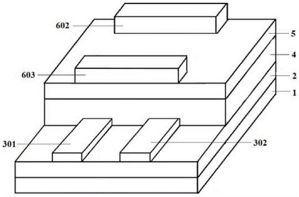
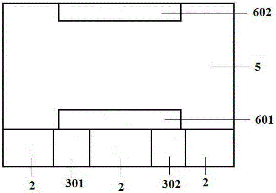
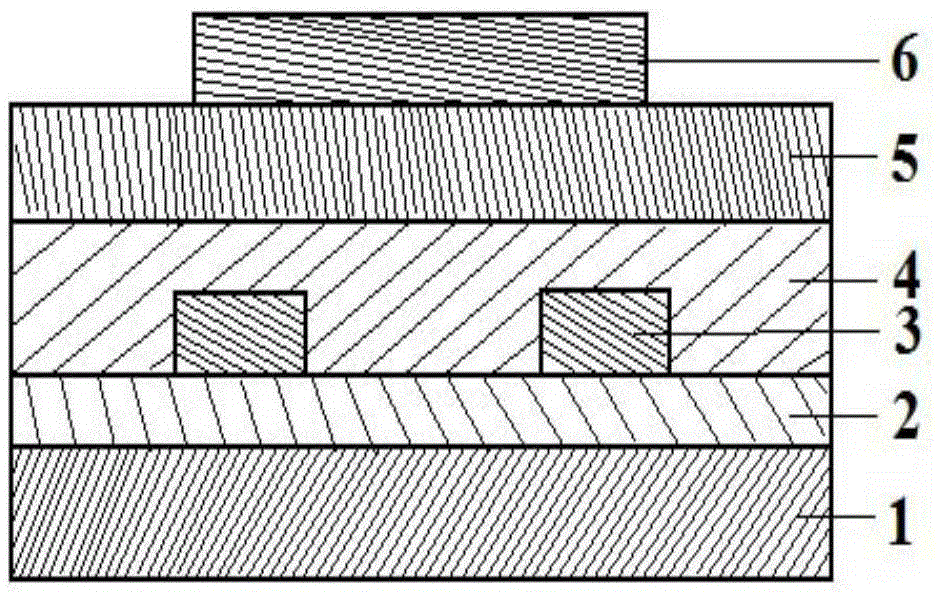
[0034] The planar separation dual-gate thin film transistor of this embodiment adopts a bottom-gate structure, and sequentially includes a substrate 1, a transition layer 2, a gate electrode layer 3, an insulating gate dielectric layer 4, a semiconductor active layer 5, and a source electrode / drain layer from bottom to top. Pole 6; the gate electrode layer is composed of two gate electrodes, and the two gate electrodes are arranged relatively parallel on the transition layer; the connection direction of the two gate electrodes is perpendicular to the source electrode / drain electrode connection direction, and its structure and Functionally equivalent; the source / drain electrodes are relatively parallel.

[0035] The substrate in this embodiment may be a glass substrate or a plastic substrate.

[0036] The semiconductor active layer in this embodiment is a 30-80 nanometer indium-doped gallium zinc oxide (IGZO) semiconductor thin film.

[0037] The insulating gate dielectric lay...


PUM


Abstract

The invention belongs to the technical field of semiconductors, and discloses a planar split dual-gate thin film transistor and a preparation method thereof. The method comprises the following steps: (1) depositing insulating medium materials on a substrate to serve as a transition layer; (2) depositing a conduction thin film on the transition layer, and carrying out photoetching to form two gate electrodes; (3) depositing insulation thin films on the transition layer and the gate electrodes to form an insulated gate medium layer; (4) depositing a thin film on the insulated gate medium layer to form a semiconductor active layer; (5) spinning a photoresist layer on the semiconductor active layer, and carrying out photoetching to form the contact hole of a source/ drain electrode; (6) depositing the conduction thin film on the contact hole and the photoresist, and stripping to form the source electrode and the drain electrode; and (7) carrying out annealing processing. The bias voltages of two gate electrodes are regulated to cause a TFT (Thin Film Transistor) device to present different output and transfer characteristics, the two gate electrodes can be simultaneously used as a control gate and a signal gate, a circuit is simplified, and the application range of the TFT is effectively expanded.

Description

technical field [0001] The invention belongs to the technical field of semiconductors, and in particular relates to a planar separation double-gate thin film transistor structure and a preparation method thereof. Background technique [0002] In recent years, thin-film transistors (TFTs) have received extensive attention and research because they are more and more widely used in flat panel displays, integrated sensors, smart identification cards, and integrated circuits. In order to meet more application requirements, TFT devices must have good device performance (high mobility, low off-state current, high switch current ratio, low threshold voltage, low sub-threshold swing, etc.) and high stability, reliability sex. Over the years, around the improvement of device performance, a variety of semiconductor thin film materials that can be used for TFT have been developed, mainly including amorphous silicon, polycrystalline silicon, organic small molecule semiconductor material...

Claims


Application Information

Patent Timeline
Patent Type & Authority Applications(China)
IPC IPC(8): H01L29/786H01L21/34
CPCH01L29/66969H01L29/78645H01L29/7869
Inventor 刘玉荣廖荣姚若河
Owner SOUTH CHINA UNIV OF TECH
Why Eureka
Try Eureka