Vertical power MOSFET cell with planar channel

A metal oxide half-field and transistor technology, which is applied in semiconductor devices, semiconductor/solid-state device manufacturing, electrical components, etc., can solve the problems of reducing efficiency and breakdown voltage, MOSFET uneven current and temperature, etc.

Active Publication Date: 2019-06-28
无锡美偌科微电子有限公司
View PDF4 Cites 0 Cited by
  • Summary
  • Abstract
  • Description
  • Claims
  • Application Information

AI Technical Summary

Problems solved by technology

Any variation between these devices may cause uneven current and temperature across the MOSFET, reducing its efficiency and breakdown voltage

Method used


Image

  • Vertical power MOSFET cell with planar channel
  • Vertical power MOSFET cell with planar channel
  • Vertical power MOSFET cell with planar channel

Examples


Embodiment Construction

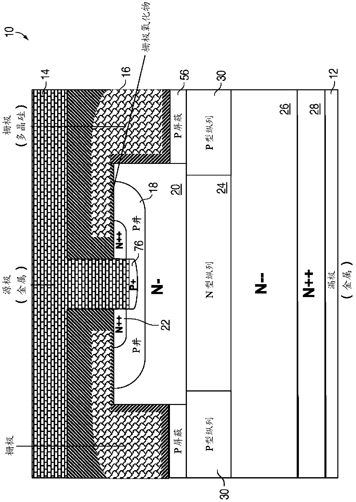
[0051] figure 1 is a cross-sectional view of a single vertical MOSFET cell 10 in a large array of identical contiguous MOSFET cells according to an embodiment of the invention. The cells shown are approximately 8-11 microns wide. The MOSFET cells 10 may have a breakdown voltage in excess of 600 volts, and the number of cells 10 in an array of the same cell determines the current handling capability, eg 20 amps. The cell array can be strip, quadrilateral, hexagonal or other existing shapes.

[0052] During normal operation, a positive voltage is applied to the bottom drain electrode 12 and a load connected between ground and the top source electrode 14 . When a positive voltage is applied to the conductive gate 16 and is greater than the threshold voltage, the top surface of the P-well 18 is inverted, and electrons accumulate along the vertical sidewalls of the N-layer 20 . The gate extends along the sidewall below the P-well 18 and creates a field plate to a lower electric ...


PUM


Abstract

The invention discloses a vertical power metal-oxide-semiconductor field-effect transistor cell with a planar channel, which comprises an N+ silicon substrate with a drain electrode. The N-type drift layer with low doping concentration is longer than the substrate. Alternate N-type columns and P-type columns are formed on the drift layer and have higher doping concentration. An N-type layer having a higher doping concentration than the drift region is then formed and etched with sidewalls. A P-well is formed in the N-type layer, and an N+ source region is formed in the P-well. A gate is formed on the lateral channel of the P-well near the sidewall to act as a vertical field plate. A source electrode contacts the P-well and the source region. A positive gate voltage inverts the lateral channel and increases conductivity along the sidewalls. The current between the source and the drain flows laterally and then vertically through various N layers. Turn-on resistance is reduced and the breakdown voltage is increased.

Description

technical field [0001] The present invention relates to power metal-oxide-semiconductor field-effect transistors (metal-oxide-semiconductor field-effect transistors, hereinafter referred to as MOSFETs), especially vertical super power transistors with planar DMOS portions and vertical conductive portions. junction MOSFET. [0002] The priority claimed by this application is the application filed by Jun Zeng et al. with the US Intellectual Property Office on February 4, 2014, and its application number is 61 / 935,707, which is hereby incorporated by reference in its entirety. Background technique [0003] Vertical MOSFETs are popular as high voltage and high power transistors due to the ability to provide a thick and low doping concentration drift layer to achieve a high breakdown voltage in the off state. Generally, the MOSFET includes a highly doped N-type substrate, a thick and low-doped N-type drift layer, a P-type body layer adjacent to the drift layer, an N-type source ...

Claims


Application Information

Patent Timeline
Patent Type & Authority Patents(China)
IPC IPC(8): H01L29/78H01L29/732H01L21/8224
CPCH01L29/407H01L29/41766H01L29/42368H01L29/66727H01L29/66734H01L29/7802H01L29/0623H01L29/0878H01L29/6634H01L29/66348H01L29/7396H01L29/0619H01L29/0834H01L29/7813H01L29/7397H01L29/4236H01L29/1095H01L29/0634H01L29/42376H01L29/7811
Inventor 曾军穆罕默德·恩·达维希蒲奎苏世宗
Owner 无锡美偌科微电子有限公司
Why Eureka
Try Eureka