CMOS device and forming method thereof

A device, anti-diffusion technology, applied in semiconductor/solid-state device manufacturing, electrical components, transistors, etc., to achieve the effect of reducing leakage current and high performance

Inactive Publication Date: 2016-03-30
SEMICON MFG INT (SHANGHAI) CORP +1
View PDF4 Cites 2 Cited by
  • Summary
  • Abstract
  • Description
  • Claims
  • Application Information

AI Technical Summary

Problems solved by technology

[0004] The present invention aims to provide a CMOS device and its forming method to solve the problem that the well structure in the CMOS device in the prior art is prone to leakage current

Method used


Image

  • CMOS device and forming method thereof
  • CMOS device and forming method thereof
  • CMOS device and forming method thereof

Examples


preparation example Construction

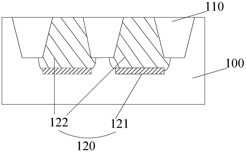
[0043] In the preparation process of the well structure, the area for forming the well structure is often set between adjacent STI structures, so as to isolate the well structures with different electrical properties and jointly form the functional area of ​​the CMOS device. The method for forming the well region structure on the substrate forming the STI structure region (STI) will be described in detail below:

[0044] First, provide the Figure 4 In the substrate 100 shown, an STI structure 110 may be pre-formed therein. Wherein, the substrate 100 may be single crystal silicon, silicon on insulator (SOI) or silicon germanium (SiGe) or the like. As an example, in this embodiment, the substrate 100 is made of single crystal silicon.

[0045] After completing the step of forming the STI structure 110 on the substrate 100, introduce anti-diffusion ions to the edge of the part of the area on the substrate 100 where the well structure 120 is to be formed (that is, the area betw...

Embodiment 1

[0050] This embodiment provides a method for manufacturing a CMOS device, comprising the following steps:

[0051] Form STI on a single crystal silicon substrate;

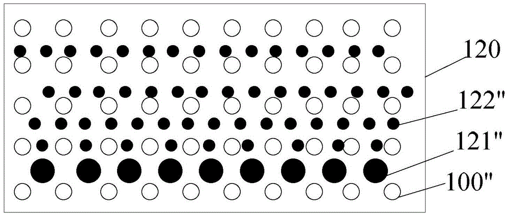
[0052] Xenon ions (Xe + ) into the substrate between some STIs, wherein the implantation energy is 500ev, and the implantation dose is 1×10 13 cm -2 , forming a depth of 500nm and a thickness of The anti-diffusion area of ​​the well area;

[0053] Using the ion implantation method of 0° tilt angle / 0° twist angle, phosphorus is doped into the substrate above the anti-diffusion region of the well region, wherein the implantation energy is 200ev, and the implantation dose is 1×10 13 cm -2 , forming an N-type doped region;

[0054] Make the P well in the same way as above, and the P type element is boron;

[0055] A CMOS device is fabricated using the above-mentioned substrate on which the N well and the P well are formed.

Embodiment 2

[0057] This embodiment provides a method for manufacturing a CMOS device, comprising the following steps:

[0058] Form STI on a single crystal silicon substrate;

[0059] Xenon ions (Xe + ) into the substrate between some STIs, wherein the implantation energy is 50000ev, and the implantation dose is 2×10 12 cm -2 , forming a depth of 500nm and a thickness of The anti-diffusion area of ​​the well area;

[0060] Using the ion implantation method of 0° tilt angle / 0° twist angle, phosphorus is doped into the substrate above the anti-diffusion region of the well region, wherein the implantation energy is 20000ev, and the implantation dose is 2×10 12 cm -2 , forming an N-type doped region;

[0061] Make the P well in the same way as above, and the P type element is boron;

[0062] A CMOS device is fabricated using the above-mentioned substrate on which the N well and the P well are formed.


PUM


Abstract

The invention discloses a CMOS device and a forming method thereof. The CMOS device comprises STI structures and well region structures located between the adjacent STI structures. Each well region structure comprises a doping region and an anti-diffusion region, wherein the doping region is disposed in a substrate, and the anti-diffusion region is disposed between the doping region and a non-doping region of the substrate, and enables the doping region and the non-doping region to be at least separated. The anti-diffusion regions are additionally disposed below the doping regions in the well region structures of the CMOS device. The pre-formed anti-diffusion regions can prevent the movement of doping ions in the subsequent doping process and the power-on application process of the device, thereby preventing the doping ions from diffusing towards the substrate from a preset well region. The leakage of the doping ions to the substrate will be correspondingly reduced based on a condition that the diffusion of the doping ions towards the substrate from the well region is limited. Moreover, the lower leakage of the doping ions facilitates the tunneling effects between the well region and the substrate even between different well regions in the subsequent use process, thereby reducing the leaked current of the CMOS device, and enabling the device to be higher in usability.

Description

technical field [0001] The invention relates to the field of semiconductor manufacturing, in particular to a CMOS device and a forming method thereof. Background technique [0002] With the development of semiconductor technology, the size of CMOS devices is required to be continuously reduced. Correspondingly, the demand for high-density, high-performance large-scale integrated circuits is also increasing. Among numerous CMOS devices, Complementary Metal Oxide (CMOS) devices, as advanced logic integrated circuits, have become the mainstream of integrated circuit development. [0003] The overall performance of a CMOS device is affected by many factors, among which the quality and performance of the well region is one of these influencing factors. Well regions of existing CMOS devices are mainly formed by high-energy ion implantation, and vertical implantation (ie, 0° tilt angle / 0° twist angle) is often used for ion implantation. However, this high-energy vertical implanta...

Claims


Application Information

Patent Timeline
Patent Type & Authority Applications(China)
IPC IPC(8): H01L27/092H01L21/8238
Inventor 叶文源
Owner SEMICON MFG INT (SHANGHAI) CORP
Why Eureka
Try Eureka