Method for forming gate structure and gate structure

A gate structure and gate technology, which is applied in the formation of gate structure and the field of gate structure, can solve the problems of complicated steps and the influence of CMOS device manufacturing, and achieve the effect of speeding up the process progress, reducing the influence, and easy etching

Active Publication Date: 2018-09-07
SEMICON MFG INT (SHANGHAI) CORP
View PDF3 Cites 0 Cited by
  • Summary
  • Abstract
  • Description
  • Claims
  • Application Information

AI Technical Summary

Problems solved by technology

[0003] Take complementary metal-oxide-semiconductor (CMOS) devices as an example. Such devices include PMOS devices and NMOS devices. Due to their different properties, these two devices have different requirements when forming gates, so they usually need to be separated in the manufacturing process. Forming gates in PMOS devices and NMOS devices, the steps are relatively complicated, which affects the production of the entire CMOS device

Method used


Image

  • Method for forming gate structure and gate structure
  • Method for forming gate structure and gate structure
  • Method for forming gate structure and gate structure

Examples


Embodiment Construction

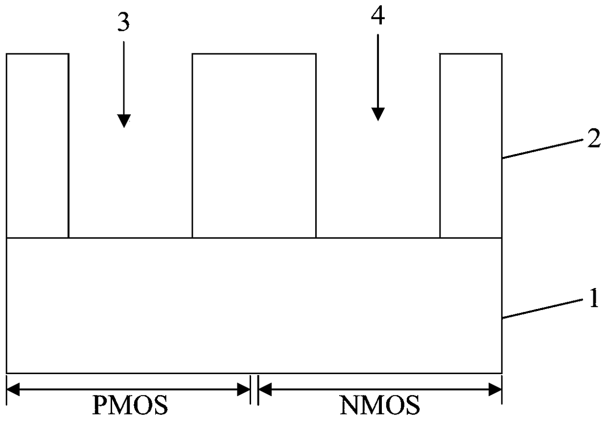
[0041] Since the properties of the PMOS device and the NMOS device are different, in the prior art, gate structures of the PMOS device and the NMOS device need to be formed separately. refer to Figure 1 to Figure 5 It is a structural schematic diagram of each step when forming a gate structure of a CMOS device in the prior art. First, refer to figure 1 A dielectric layer 2 having openings 3 and 4 is formed on the substrate 1, and the openings 3 and 4 are used to respectively form gate structures of PMOS devices and NMOS devices in subsequent steps.

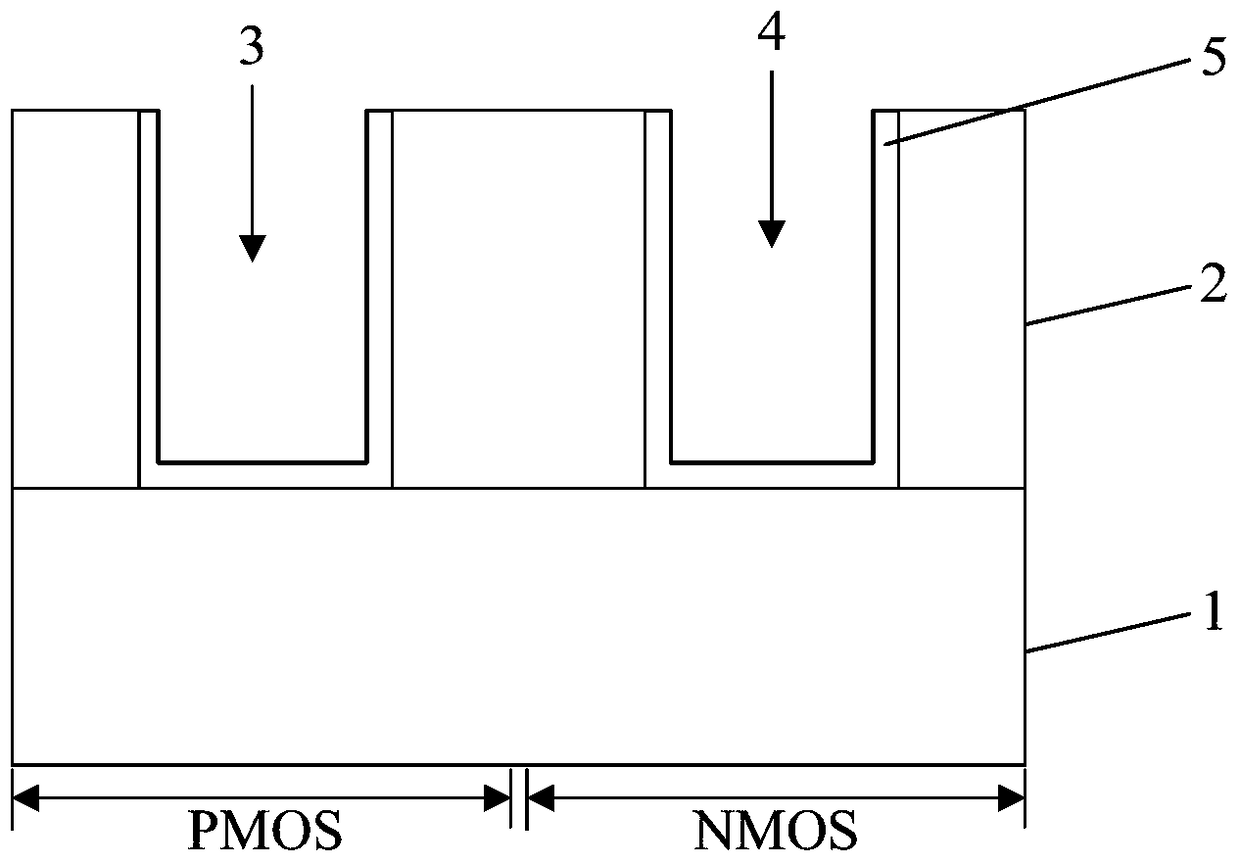
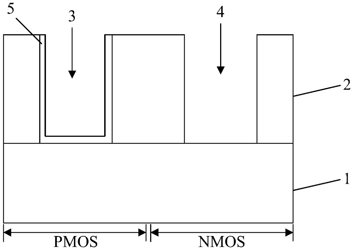
[0042] continue to refer figure 2 as well as image 3 , forming a PMOS work function layer 5 in the openings 3 and 4, and then removing part of the PMOS work function layer 5, leaving only the PMOS work function layer 5 in the opening 3 corresponding to the PMOS region. Specifically, in the prior art, an etching mask such as photoresist is generally formed on the PMOS work function layer 5 that needs to be preserved, and the ...


PUM


Abstract

The invention provides a method of forming a gate structure and a gate structure. The method of forming the gate structure comprises the steps of providing a substrate, forming a dielectric layer on the substrate, and forming a first opening and a second opening in the dielectric layer; forming a first work function layer; reserving only the first work function layer in the first opening to forming a work function layer of an NMOS device; respectively forming second work function layers in the second opening and on the first work function layer in the first opening; and forming a gate. The gate structure comprises the substrate, the dielectric layer, and the first and second openings located in the dielectric layer; and the first work function layer, the second work function layer and the gate. The invention has the beneficial effects of facilitating the acceleration of the progress of the process and reducing effects on other semiconductor devices during the etching by first forming the work function layer of the NMOS device; eliminating the process of forming a diffusion barrier layer; and increasing the space of the first and second openings thereby facilitating the formation of the gate.

Description

technical field [0001] The invention relates to the field of semiconductor manufacturing, in particular to a method for forming a gate structure and the gate structure. Background technique [0002] With the continuous advancement of semiconductor technology, the feature size of semiconductor devices is gradually reduced. The gradual reduction of the feature size of semiconductor devices puts forward higher requirements for the semiconductor manufacturing process. [0003] Take complementary metal-oxide-semiconductor (CMOS) devices as an example. Such devices include PMOS devices and NMOS devices. Due to their different properties, these two devices have different requirements when forming gates, so they usually need to be separated in the manufacturing process. The steps of forming gates in PMOS devices and NMOS devices are relatively complicated, which affects the fabrication of the entire CMOS device. [0004] Therefore, how to simplify and speed up the process of formi...

Claims


Application Information

Patent Timeline
Patent Type & Authority Patents(China)
IPC IPC(8): H01L27/092H01L21/8238
Inventor 徐建华张子莹
Owner SEMICON MFG INT (SHANGHAI) CORP
Why Eureka
Try Eureka