
An electron bombardment solid-state photomultiplier tube type low-light digital image sensor
A photomultiplier tube, digital image technology, applied in the direction of image communication, television, electrical components, etc., can solve the problems of inability to realize gating working mode, no electronic shutter function, large sensor power consumption, etc., and achieve high time resolution capability, The effect of light weight and fast frame transfer rates
- Summary
- Abstract
- Description
- Claims
- Application Information
AI Technical Summary
Problems solved by technology
Method used
Image

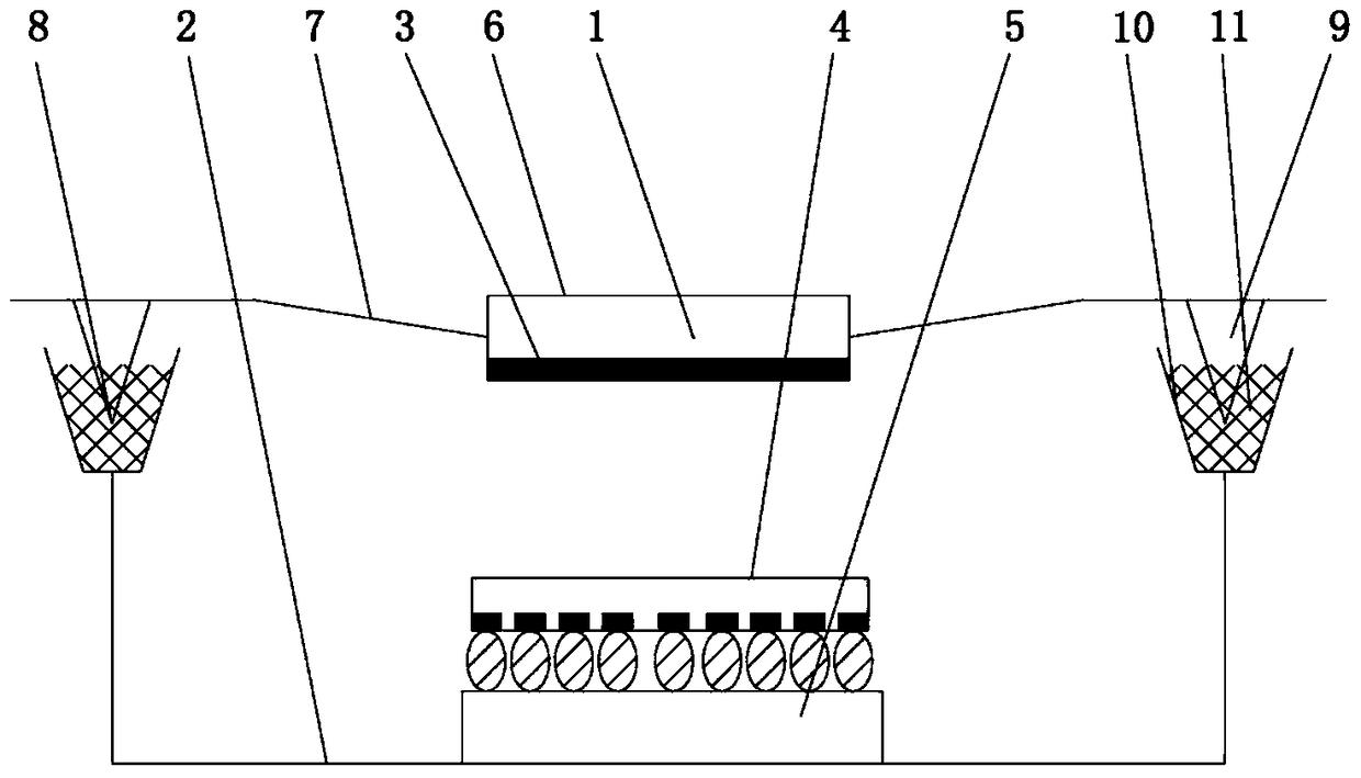
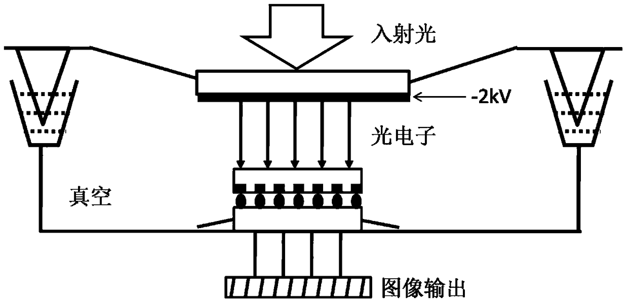
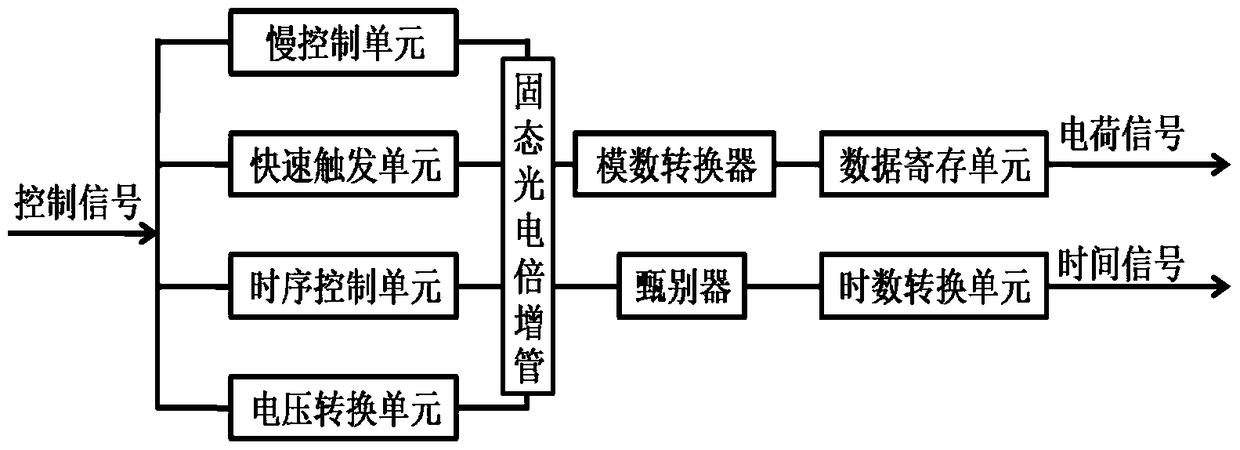
Examples
Embodiment Construction
[0033] Recently, a new type of photodetection device, the solid-state photomultiplier tube, has gradually attracted attention. For specific technologies, please refer to documents such as Nuclear Instruments and Methods in Physics Research A 567 (2006) 48-56. The solid-state photomultiplier tube consists of an array of hundreds or thousands of avalanche diodes operating in Geiger mode, and each avalanche diode cell is connected in series with a quenching resistor. In the case of reverse voltage bias, the depletion layer of each microcell has a high electric field. When the incident photon hits the microcell area, electron-hole pairs are generated inside the semiconductor. These electrons and holes are in the Under the action of the electric field, more secondary electrons and holes will be generated, resulting in an avalanche effect. At this time, the current in each micro-element circuit increases, forming a large voltage drop on the quenching resistor, and outputting an inst...
PUM
 Abstract
Description
Claims
Application Information