A kind of lead solder solder for semiconductor power device packaging and its preparation method and application

A technology of wire welding and power devices, which is applied in the direction of semiconductor devices, welding equipment, electric solid devices, etc., can solve the problems of excessive diffusion depth and warpage, and achieve the effects of reducing welding defects, improving density and excellent welding effect

Active Publication Date: 2018-06-01
王伟
View PDF6 Cites 0 Cited by
  • Summary
  • Abstract
  • Description
  • Claims
  • Application Information

AI Technical Summary

Problems solved by technology

If this point is ignored, many problems will be caused, such as warping caused by thermal stress, continuous diffusion caused by higher than the diffusion temperature, making the diffusion depth exceed the product setting value, etc.

Method used


Image

  • A kind of lead solder solder for semiconductor power device packaging and its preparation method and application
  • A kind of lead solder solder for semiconductor power device packaging and its preparation method and application
  • A kind of lead solder solder for semiconductor power device packaging and its preparation method and application

Examples


Embodiment 1

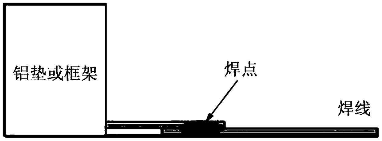
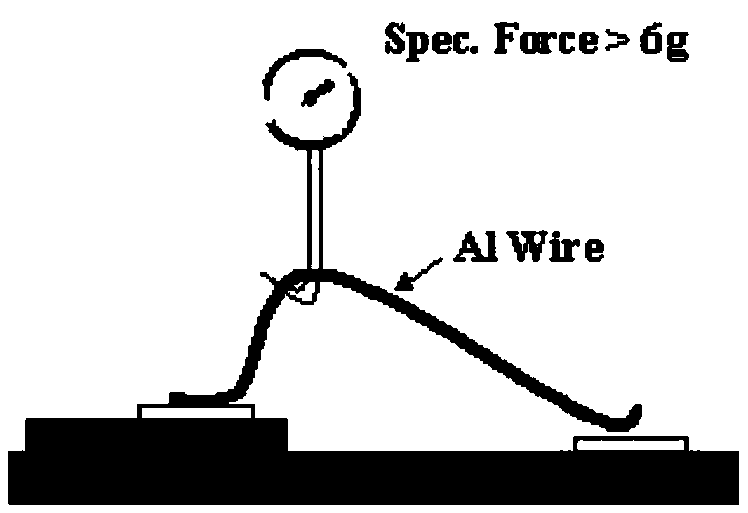
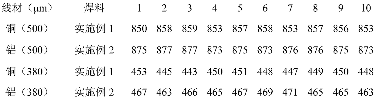
[0056] This embodiment is the soft soldering of copper wire and chip aluminum pad, and copper wire and frame, adopts solder A to carry out welding, and its chemical composition is (wt.%): Sn 34.1%, Cu 22.4%, Al 20 %, Ag 2.0%, Bi 3.5%, Sb 9.0%, In 9.0%.

[0057] The copper wire and the aluminum pad of the chip are welded to form the first solder joint, the preheating temperature is 220°C, the welding temperature is 290°C, the copper wire is welded to the copper frame to form the second solder joint, the preheating temperature is 220°C, and the welding temperature is 300°C.

Embodiment 2

[0061] This embodiment is the soft soldering of copper wire and chip aluminum pad, and copper wire and frame, adopts solder A to carry out welding, and its chemical composition is (wt.%): Cu 23.1%, Al 18.7%, Ag 3.5 %, Bi 3.5%, Sb 8.3%, In 8.0%, Sn balance.

[0062] The copper wire and the aluminum pad of the chip are welded to form the first solder joint, the preheating temperature is 220°C, the welding temperature is 290°C, the copper wire is welded to the copper frame to form the second solder joint, the preheating temperature is 220°C, and the welding temperature is 300°C.

Embodiment 3

[0066] This embodiment is the soldering of aluminum welding wire and chip aluminum pad, and aluminum welding wire and frame, adopts solder B to carry out welding, and its chemical composition is (wt.%): Sn 34.1%, Cu 21.0%, Al 23.4 %, Ag 2.0%, Bi 3.5%, Sb 8.0%, In 8.0%.

[0067] The aluminum wire is welded to the chip aluminum pad to form the first solder joint: the preheating temperature is 220°C, and the welding temperature is 290°C. The aluminum welding wire is welded with the copper frame to form the second solder joint: the preheating temperature is 220°C, and the welding temperature is 300°C.


PUM

PropertyMeasurementUnit
diameteraaaaaaaaaa
strengthaaaaaaaaaa
thicknessaaaaaaaaaa

Abstract

The invention discloses lead welding brazing filler metal for packaging of a semiconductor power device and a preparation method and application thereof, and belongs to the technical field of packaging and manufacturing of semiconductor power devices. The brazing filler metal is brazing filler metal for a copper or aluminum lead; the brazing filler metal for the copper lead (wt.%) comprises 20-29% of Cu, 10.0-20.0% of Al, 2.0-11.0% of Ag, 2.0-5.0% of Bi, 3.0-9.0% of Sb, 3.0-9.0% of In and the balance of Sn; and the brazing filler metal for the aluminum lead (wt.%) comprises 21.0-29.0% of Cu, 18.0-27% of Al, 2.0-9.0% of Ag, 2.0-3.5% of Bi, 6.0-8.0% of Sb, 6.0-8.0% of In and the balance of Sn. In a lead welding process of the brazing filler metal for packaging of the semiconductor power device, the welding temperature is 280-320 DEG C to directly melt and moisten an aluminum pad and a frame to realize stable and reliable connection among the three.

Description

technical field [0001] The invention relates to the technical field of packaging and manufacturing of semiconductor power devices, in particular to a lead solder for semiconductor power device packaging and its preparation method and application. Background technique [0002] In nature, the electrical conductivity and thermal conductivity of copper are second only to silver, and the affinity between copper and humans is second only to titanium. Therefore, copper has been widely used in the fields of electricity transmission, heat exchange and daily necessities. Applications. [0003] In the packaging and manufacturing process of semiconductor power devices, considering the characteristics of high current, high calorific value and ultra-high power of power devices, it is decided to use copper instead of or partially replace aluminum wires to complete the connection between chips and pins, and the most critical link , that is to realize the stable connection between the coppe...

Claims


Application Information

Patent Timeline
Patent Type & Authority Patents(China)
IPC IPC(8): B23K35/26C22C13/00C22C30/04C22C1/02C22F1/16
CPCB23K35/262C22C1/02C22C13/00C22C30/04C22F1/16H01L2224/45124H01L2224/48091H01L2224/48227H01L2224/48472H01L2224/85203H01L2224/859H01L2924/00014
Inventor 王伟
Owner 王伟
Why Eureka
Try Eureka