EUV design rule, light source and mask joint optimization method and imaging modeling method

A joint optimization and imaging model technology, applied in the field of extreme ultraviolet lithography imaging modeling, can solve problems such as there is no EUV lithography SMO method

Active Publication Date: 2016-05-11
INST OF MICROELECTRONICS CHINESE ACAD OF SCI
View PDF4 Cites 21 Cited by
  • Summary
  • Abstract
  • Description
  • Claims
  • Application Information

AI Technical Summary

Problems solved by technology

Compared with 193nm lithography technology, although EUV lithography technology has a great advantage in terms of resolution, it also meets new challenges in lithography simulation and optimization. At present, the industry does not have a practical solution for EUV lithography. The SMO method

Method used


Image

  • EUV design rule, light source and mask joint optimization method and imaging modeling method
  • EUV design rule, light source and mask joint optimization method and imaging modeling method
  • EUV design rule, light source and mask joint optimization method and imaging modeling method

Examples


Embodiment Construction

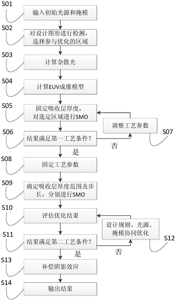
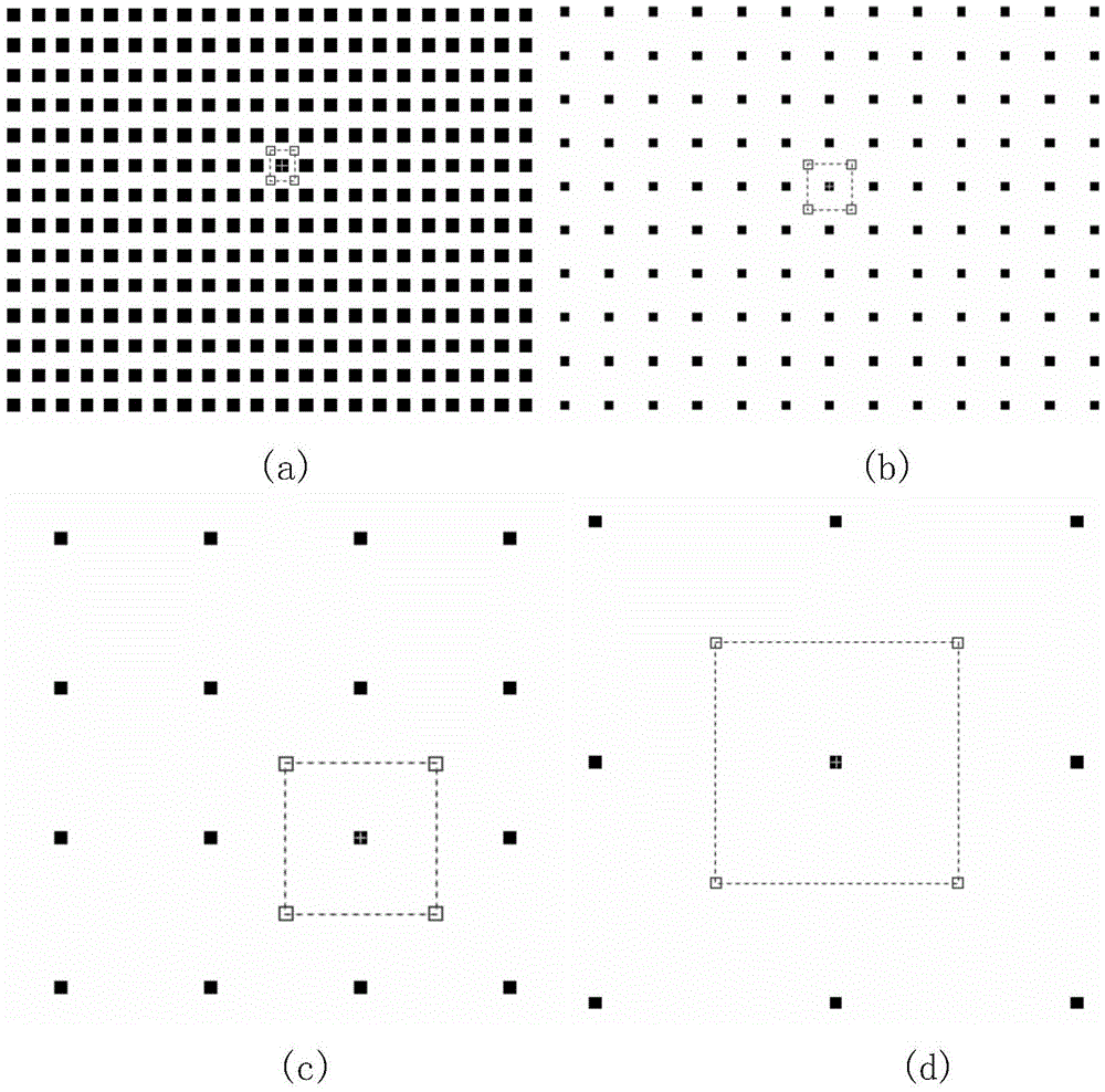
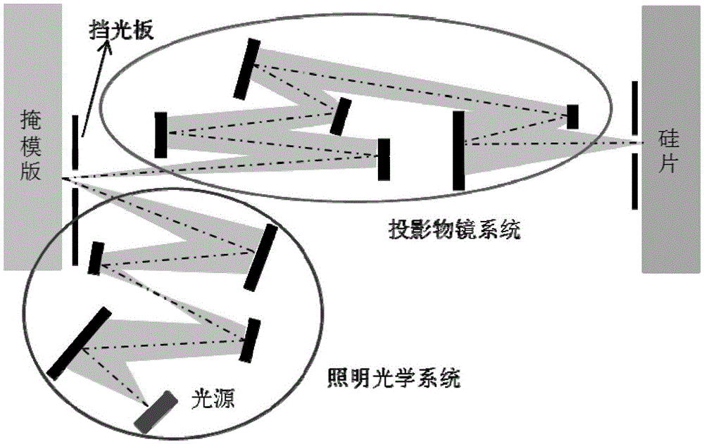
[0044] Hereinafter, embodiments of the present disclosure will be described with reference to the drawings. It should be understood, however, that these descriptions are exemplary only, and are not intended to limit the scope of the present disclosure. Also, in the following description, descriptions of well-known structures and techniques are omitted to avoid unnecessarily obscuring the concept of the present disclosure.

[0045] Various structural schematic diagrams according to embodiments of the present disclosure are shown in the accompanying drawings. The figures are not drawn to scale, with certain details exaggerated and possibly omitted for clarity of presentation. The shapes of the various regions and layers shown in the figure, as well as their relative sizes and positional relationships are only exemplary, and may deviate due to manufacturing tolerances or technical limitations in practice, and those skilled in the art will Regions / layers with different shapes, s...


PUM


Abstract

The invention discloses an extreme ultraviolet (EUV) design rule, light source and mask joint optimization method. The EUV design rule, light source and mask joint optimization method comprises the steps of conducting primary optimization simulation aiming at a provided EUV model, and acquiring a light source and a mask layout which meet the first photolithography technique condition; conducting secondary optimization simulation, and acquiring an optimal design rule, an optimal light source and an optimal mask layout which meet the second photolithography technique condition. The invention further discloses an EUV photoetching imaging modeling method. According to the EUV photoetching imaging modeling method, a chip design rule is optimized and introduced into the SMO process to obtain a design objective graph and advanced SMO joint optimization method, part of device layout line widths and intervals are adjusted slightly on the premise that the device size is unchanged, and then the whole process window is increased, optimization time is shortened and the compound process window is also increased.

Description

technical field [0001] The invention relates to the technical field of semiconductor manufacturing, in particular to a joint optimization method for design rules, a light source, and a mask in extreme ultraviolet lithography (EUV), and an imaging modeling method for extreme ultraviolet lithography. Background technique [0002] Lithography is the most important part of the chip manufacturing process, and since lithography is the only process step that produces patterns, it is the main driving force of Moore's Law. At present, the lithography process of the 14nm node is realized by the 193nm immersion lithography system combined with the double pattern exposure technology, and the industry expects that the 10nm and below nodes will be realized by the multiple exposure technology. However, double-pattern exposure and multiple-pattern methods will bring problems such as cumbersome design rules, complex processes, and sharply increased production costs. With the further advancem...

Claims


Application Information

Patent Timeline
IPC IPC(8): G06F17/50G03F1/22
CPCG03F1/22G06F30/20G06F30/39G06F30/398G06F2119/18
Inventor 郭沫然宋之洋韦亚一
Owner INST OF MICROELECTRONICS CHINESE ACAD OF SCI
Why Eureka
Try Eureka