How the transistor is formed

A transistor and stress layer technology, applied in semiconductor devices, semiconductor/solid-state device manufacturing, electrical components, etc., can solve problems such as poor conductivity and large series contact resistance, and achieve enhanced conductivity, reduced series contact resistance, and reduced interface. The effect of the barrier

Active Publication Date: 2019-03-12
SEMICON MFG INT (SHANGHAI) CORP
View PDF2 Cites 0 Cited by
  • Summary
  • Abstract
  • Description
  • Claims
  • Application Information

AI Technical Summary

Problems solved by technology

However, the series contact resistance at the interface between the metal silicide layer 04 and the stress layer made according to the prior art is relatively large, so that the conductivity between the conductive plug and the source electrode, and between the conductive plug and the drain electrode is relatively poor.

Method used


Image

  • How the transistor is formed
  • How the transistor is formed
  • How the transistor is formed

Examples


Embodiment Construction

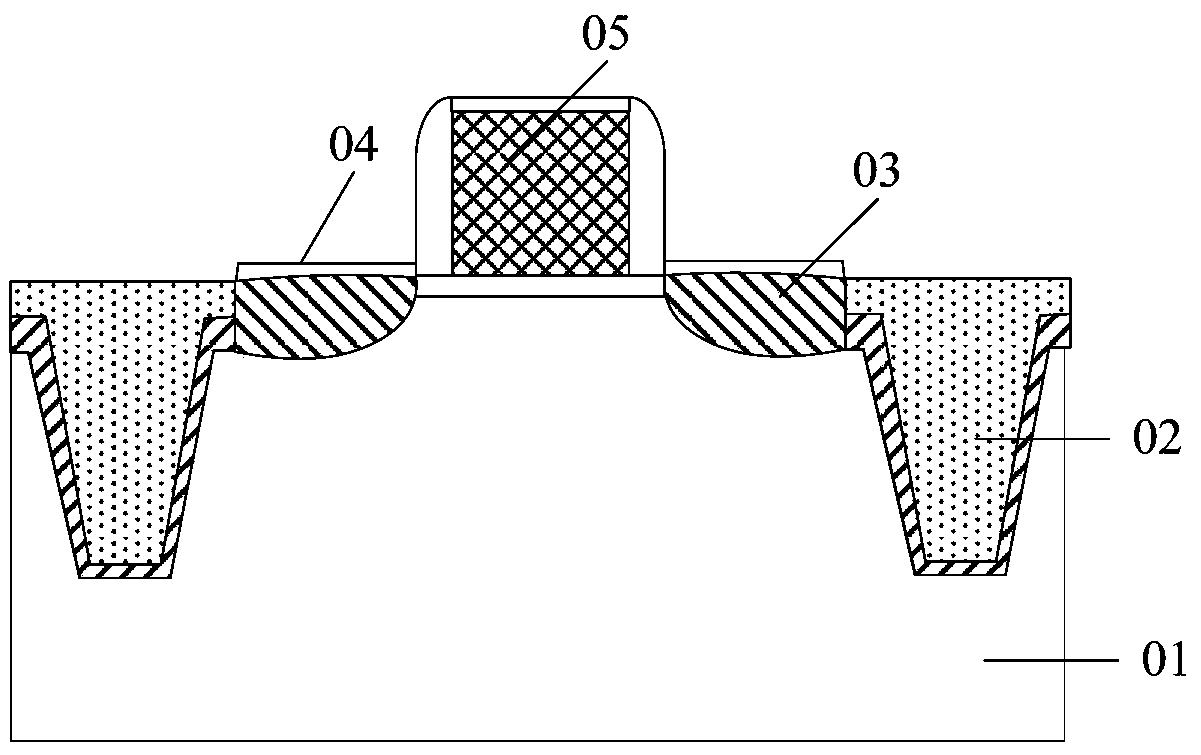
[0037] As described in the background, in prior art transistors, the quality of the metal silicide layer on the stress layer is poor and the resistance is high, and the series contact resistance at the interface between the metal silicide layer and the stress layer is relatively large, so that the conductive plug The conductivity between the source, the conductive plug and the drain is poor.

[0038] Analyze the reasons for the large series contact resistance at the interface between the metal silicide layer and the stress layer, continue to refer to figure 1 As shown, the usual method of forming the metal silicide layer 04 is to form a metal material layer on the SiC stress layer 03 and anneal the metal material layer. During the annealing process, the metal atoms in the metal material layer diffuse into the SiC stress layer Inside 03, it reacts with the silicon atoms in the SiC stress layer 03 to form a metal silicide layer 04. Due to the existence of carbon atoms in the Si...


PUM


Abstract

The invention provides a forming method of a transistor. The forming method comprises the steps of forming recessed troughs on a substrate at positions at two sides of a gate electrode; forming stress layers in the recessed troughs, performing doping on the stress layer and forming a source electrode and a drain electrode; performing five-family ion implantation on the stress layer, wherein the implanted five families of ions comprise one or two kinds of antimony ion and bismuth ion, and forming a metal silicide layer on the stress layer. The atomic radius of the antimony ion or the bismuth ion is relatively large, thereby realizing no easy migration in an annealing process. Therefore, in the annealing process and a subsequent process, the antimony ions or the bismuth ions can be easily kept at an interface between the metal silicide layer and the stress layer, thereby reducing an interface barrier between the metal silicide layer and the stress layer, furthermore reducing a series contact resistance at the interface between the metal silicide layer and the stress layer, and improving conductivity at a part between a subsequently formed conductive plug and the source electrode and a part between the conductive plug and the drain electrode.

Description

technical field [0001] The invention relates to the field of semiconductors, in particular to a method for forming a transistor. Background technique [0002] In the field of semiconductors, stress technology can provide tensile stress or compressive stress to the channel region, so as to achieve the effect of improving the carrier mobility of CMOS devices, and then improve the performance of transistors. [0003] For example: forming a groove in the substrate corresponding to the source region and the drain region of the PMOS transistor, then epitaxially growing a silicon germanium layer in the groove, performing ion implantation on the silicon germanium layer to form the source region and the drain region, the The silicon germanium layer can apply compressive stress to the channel of the PMOS transistor. A groove is also formed in the substrate corresponding to the source region and the drain region of the NMOS transistor, a SiC layer is formed in the groove, and ion impl...

Claims


Application Information

Patent Timeline
Patent Type & Authority Patents(China)
IPC IPC(8): H01L21/336H01L21/28H01L21/768
Inventor 周祖源
Owner SEMICON MFG INT (SHANGHAI) CORP
Why Eureka
Try Eureka