Semiconductor structure and formation method thereof
A technology of semiconductor and gate structure, applied in the field of semiconductor structure and its formation, can solve problems such as gate leakage
- Summary
- Abstract
- Description
- Claims
- Application Information
AI Technical Summary
Problems solved by technology
Method used
Image

Examples
Embodiment Construction
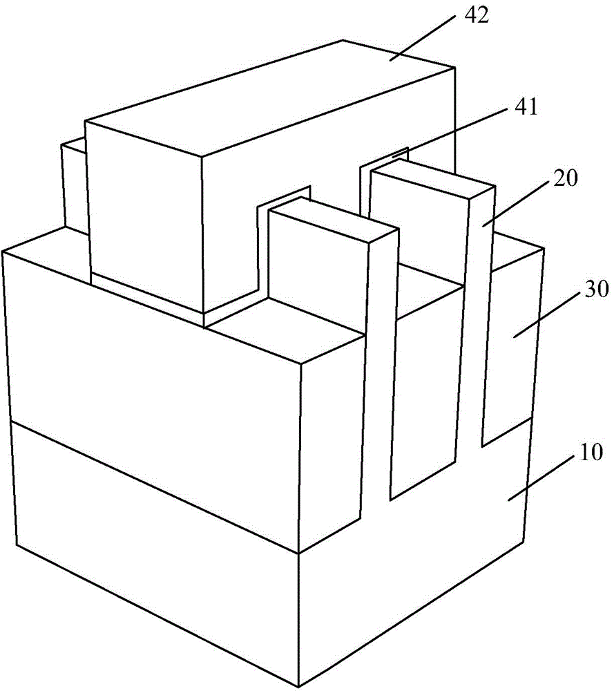
[0030] As mentioned in the background, the gate leakage phenomenon often occurs in the existing FinFET, which reduces the reliability of the FinFET.
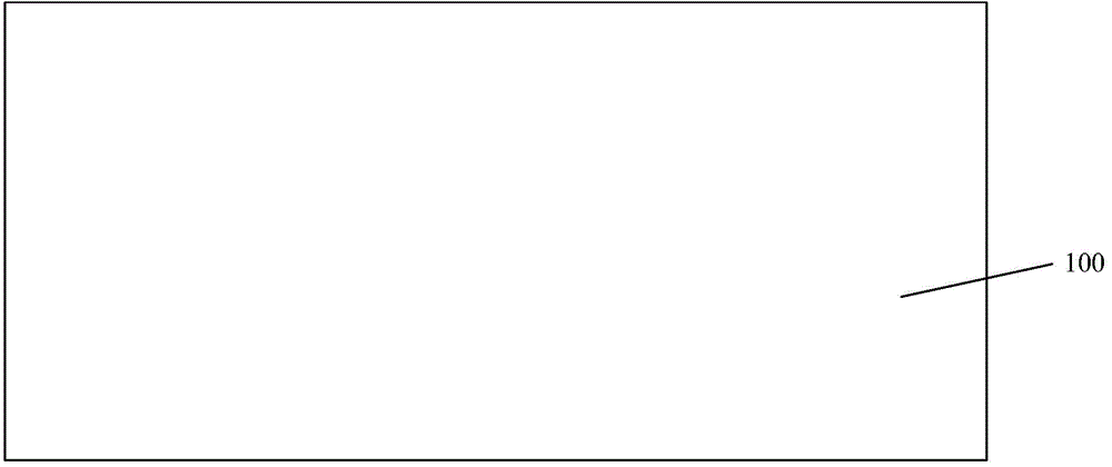
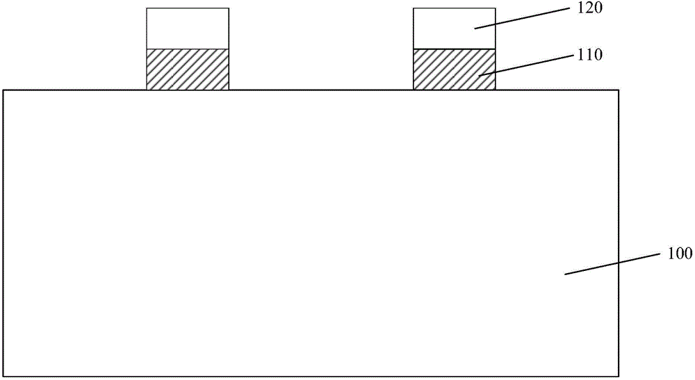
[0031] In the prior art, the fin portion of the fin field effect transistor is usually formed by etching the semiconductor substrate, and a mask layer and a patterned photoresist layer located on the surface of the mask layer are formed on the semiconductor substrate, and the pattern The patterned photoresist layer defines the size and position of the formed fin; then the patterned photoresist layer is used as a mask to etch the mask layer, and the pattern of the photoresist layer is transferred to the mask layer; and then The semiconductor layer is etched using the mask layer as a mask to form fins. Since the patterned photoresist layer is formed by exposing and developing the photoresist layer, the edges of the patterned photoresist layer are generally rough; thus the edges of the pattern transferred to the mask layer are also...
PUM
 Abstract
Description
Claims
Application Information
 - R&D
- Intellectual Property
- Life Sciences
- Materials
- Tech Scout
- Unparalleled Data Quality
- Higher Quality Content
- 60% Fewer Hallucinations
Browse by: Latest US Patents, China's latest patents, Technical Efficacy Thesaurus, Application Domain, Technology Topic, Popular Technical Reports.
© 2025 PatSnap. All rights reserved.Legal|Privacy policy|Modern Slavery Act Transparency Statement|Sitemap|About US| Contact US: help@patsnap.com