
A method for manufacturing fine lines in the inner layer of a printed circuit board

A printed circuit board and fine circuit technology, which is applied in the fields of printed circuit manufacturing, circuit lamination, printed circuit, etc., can solve the problem of poor bonding between substrate and conductive layer, incomplete avoidance of side erosion, long production cycle, etc. problems, to achieve the effect of solving poor bonding force, shortening production cycle, and solving side erosion problems

Active Publication Date: 2018-09-11
BOMIN ELECTRONICS CO LTD +1
View PDF9 Cites 0 Cited by
  • Summary
  • Abstract
  • Description
  • Claims
  • Application Information

AI Technical Summary

Problems solved by technology

Although this method solves the problem of side etching to a large extent, it requires two steps of film application, exposure, and development. The process is complicated and the production cycle is long. In addition, there is a flash etching process in this method, which does not completely avoid the side etching phenomenon. In addition, this method directly deposits copper on the substrate, which will eventually lead to the problem of poor bonding between the substrate and the conductive layer

Method used


Image

  • A method for manufacturing fine lines in the inner layer of a printed circuit board
  • A method for manufacturing fine lines in the inner layer of a printed circuit board
  • A method for manufacturing fine lines in the inner layer of a printed circuit board

Examples


Embodiment 1

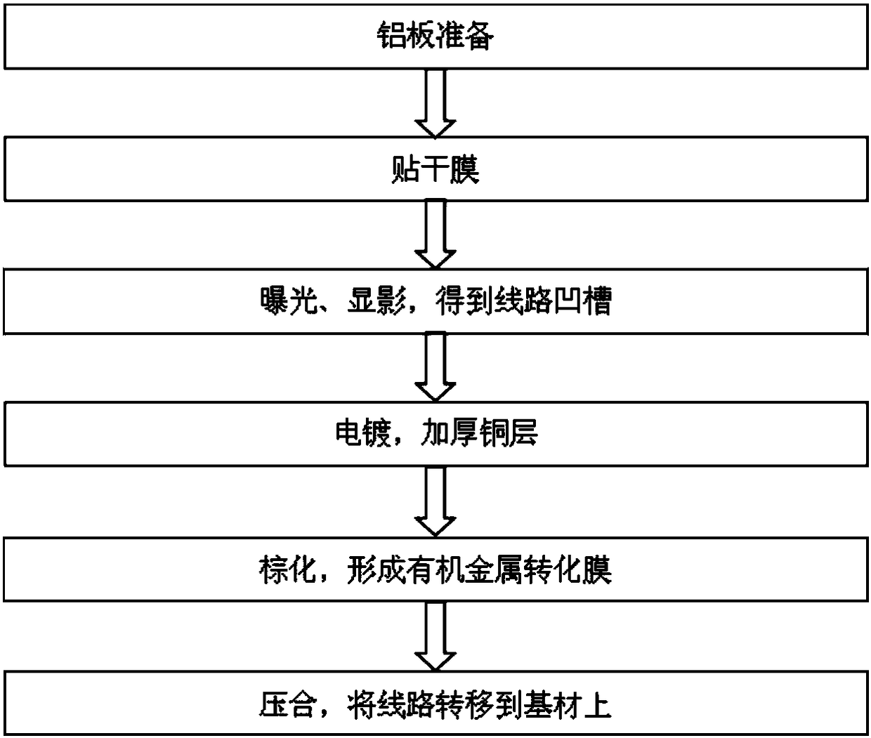
[0044] A method for manufacturing fine lines in the inner layer of a printed circuit board, comprising the steps of:

[0045] (1) Stick a layer of acid-resistant photoresist dry film with a thickness of 20 μm on the aluminum plate; before sticking the film, roughen the surface of the aluminum plate, specifically using H 2 SO 4 and H 2 o 2 The composition of the mixed solution washes the surface of the aluminum plate for 30 seconds; where H 2 SO 4 The concentration is 120g / L, H 2 o 2 The concentration is 12g / L. The roughening treatment makes the photoresist dry film and the aluminum plate tightly bonded.

[0046] (2) Use the LDI laser direct imaging exposure machine for exposure processing to obtain the conductive circuit pattern; in the exposure processing, follow the positive film process, and the unexposed part is the circuit area.

[0047] (3) developing process, the developing solution used is K 2 CO 3 solution, the K 2 CO 3 The concentration of the solution is...

Embodiment 2

[0052] A method for manufacturing fine lines in the inner layer of a printed circuit board, comprising the steps of:

[0053] (1) Stick a layer of acid-resistant photoresist dry film with a thickness of 30 μm on the aluminum plate; before sticking the film, roughen the surface of the aluminum plate, specifically using H 2 SO 4 and H 2 o 2 The composition of the mixed solution washes the surface of the aluminum plate for 180 seconds; where H 2 SO 4 The concentration is 70g / L, H 2 o 2 The concentration is 6g / L. Make the photoresist dry film and the aluminum plate tightly bonded.

[0054] (2) Use the LDI laser direct imaging exposure machine for exposure processing to obtain the conductive circuit pattern; in the exposure processing, follow the positive film process, and the unexposed part is the circuit area.

[0055] (3) developing process, the developing solution used is K 2 CO 3 solution, the K 2 CO 3 The concentration of the solution is 1.3%, and the developing t...

Embodiment 3

[0060] A method for manufacturing fine lines in the inner layer of a printed circuit board, comprising the steps of:

[0061] (1) Paste a layer of acid-resistant photoresist dry film with a thickness of 40 μm on the aluminum plate; before the film, roughen the surface of the aluminum plate, specifically using H 2 SO 4 and H 2 o 2 The composition of the mixed solution washes the surface of the aluminum plate for 100 seconds; where H 2 SO 4 The concentration is 90g / L, H 2 o 2 The concentration is 9g / L. Make the photoresist dry film and the aluminum plate tightly bonded.

[0062] (2) Use the LDI laser direct imaging exposure machine for exposure processing to obtain the conductive circuit pattern; in the exposure processing, follow the positive film process, and the unexposed part is the circuit area.

[0063] (3) developing process, the developing solution used is K 2 CO 3 solution, the K 2 CO 3 The concentration of the solution is 1%, and the developing time is 2 mi...


PUM


Abstract

The invention discloses a method for manufacturing fine lines in the inner layer of a printed circuit board; it belongs to the technical field of printed circuit board production; its technical points include the following steps: (1) pasting a layer of photoresist dry film on an aluminum plate (2) Exposure treatment to obtain the conductive circuit pattern; (3) Development treatment to obtain the circuit groove; (4) Electroplating to obtain the copper circuit with the required thickness; (5) Browning to make the surface of the copper circuit rough and form a (6) pressing, transferring the circuit on the aluminum plate to the prepreg by pressing, and completing the production of the fine circuit in the inner layer; The invention relates to a method for manufacturing fine inner layers of printed circuit boards, which is used for manufacturing fine inner layers of printed circuit boards.

Description

technical field [0001] The invention relates to a process for preparing a printed circuit board, and more specifically, to a method for manufacturing a fine circuit in an inner layer of a printed circuit board. Background technique [0002] The development trend of miniaturization of electronic products promotes the development of circuit boards in a more precise direction. The transmission of electrical signals in the circuit board is mainly realized through lines, so the degree of refinement of the lines determines the miniaturization degree of the circuit board to a large extent. The methods of circuit production mainly include subtractive method, semi-additive method, and full-additive method. In the process of manufacturing circuits by the subtractive method, serious problems such as side etching and unclean etching will be caused, and thinner circuits cannot be manufactured. The semi-additive method reduces the undercut to a large extent and can be used in the produc...

Claims


Application Information

Patent Timeline
Patent Type & Authority Patents(China)
IPC IPC(8): H05K3/20H05K3/38
CPCH05K3/205H05K3/385H05K2203/06H05K2203/11
Inventor 何慧蓉陈际达张胜涛陈世金廖敏会李灵星胡志强邓宏喜徐缓
Owner BOMIN ELECTRONICS CO LTD
Learn More