A kind of cmos circuit based on flexible thin film transistor and its manufacturing method

A thin film transistor and flexible thin film technology, which is applied in the field of semiconductor device and circuit manufacturing, can solve the problems of limited device size, small-sized device fabrication and uniformity, etc., so as to reduce process complexity and cost, improve uniformity and high gain. Effect

Active Publication Date: 2019-04-23
SUZHOU INST OF NANO TECH & NANO BIONICS CHINESE ACEDEMY OF SCI
View PDF2 Cites 0 Cited by
  • Summary
  • Abstract
  • Description
  • Claims
  • Application Information

AI Technical Summary

Problems solved by technology

[0002] Printed electronic devices come from the emerging printed electronic technology. Although they are not as good as silicon-based semiconductor microelectronic devices in performance, due to their simple printing process and non-selectivity to substrate materials, they can be used in large areas and flexible , The application field of low-cost electronic devices has the incomparable advantages of silicon-based semiconductor microelectronics
One of the most serious problems currently facing silicon-based electronics is the fabrication and uniformity of small-sized devices caused by the device size being limited by the silicon material's own structure.

Method used


Image

  • A kind of cmos circuit based on flexible thin film transistor and its manufacturing method
  • A kind of cmos circuit based on flexible thin film transistor and its manufacturing method
  • A kind of cmos circuit based on flexible thin film transistor and its manufacturing method

Examples


Embodiment 1

[0030] Example 1: A semiconductor carbon nanotube CMOS inverter with a top-gate structure and its preparation.

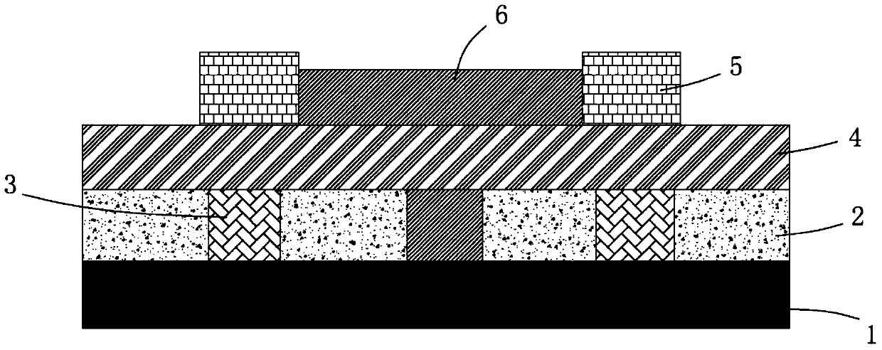
[0031] Such as figure 1 Shown is a carbon nanotube CMOS inverter with atomically deposited hafnium oxide of a certain thickness as the gate dielectric 4 and nano-silver as the top gate 5 . The source and drain electrodes 2 of the two transistors are all gold electrodes deposited by electron beam evaporation, and the channel region between each source and drain electrode is a semiconducting carbon nanotube 3 deposited by printing, forming two complete bipolar Sexual transistor devices.

[0032] Connect the drain electrode of one of the transistors to the drain electrode of the other transistor, and its potential is the output voltage (Vout) of the inverter. Connect the gates 5 of the two transistors with a conductive material 6, and its voltage is used as the input voltage (Vin), thus forming a CMOS inverter circuit. The schematic diagram of the inverter can be fou...

Embodiment 2

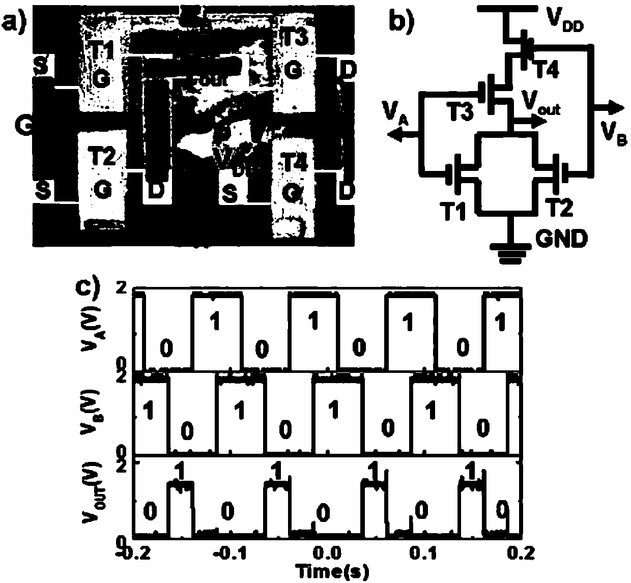
[0040] Example 2: Carbon nanotube CMOS NOR gate circuit with top gate structure

[0041] Such as image 3 As shown, adopt the step of embodiment 1 to prepare a plurality of bipolar field effect transistors, and according to image 3 As shown in (a) and (b), the source, drain and gate electrodes are connected to obtain an undoped CMOS NOR gate circuit based on carbon nanotubes. When V 1 =VDD,V 2 When =GND, the logic circuit realizes the NOR gate logic function. NOR gate is when two signal sources V A , V B When both are low level (0,0), the output is high level 1, as long as one is high level 1, then the output is low level 0. Depend on image 3 As shown in (c), it exhibits a good NOR logic function.

Embodiment 3

[0042] Embodiment 3: Carbon nanotube CMOS ring oscillator with top gate structure


PUM


Abstract

The application discloses a flexible-film-transistor-based CMOS circuit and a manufacturing method thereof. The CMOS circuit comprises a flexible substrate and a plurality of bipolar field-effect film transistors formed on the flexible substrate; an active conducting layer of each bipolar field-effect film transistor employs a carbon nano tube; and the plurality of bipolar field-effect film transistors are connected electrically to form a CMOS circuit. According to the invention, an inverter with high stability and high gain is prepared on the flexible substrate by means of printing; the process complexity and cost of the CMOS circuit manufacturing are substantially reduced; the device performance uniformity is improved; and a novel design concept and an effective implementation method are provided for a large-scale integrated wiener circuit.

Description

technical field [0001] The present invention relates to a method of manufacturing semiconductor devices and circuits, and more particularly, the present invention relates to methods of manufacturing inverters, ring oscillators, and simple logic circuits using printing to build complementary semiconductor transistor structures. Background technique [0002] Printed electronic devices come from the emerging printed electronic technology. Although the performance is not as good as silicon-based semiconductor microelectronic devices, due to its simple printing process and non-selectivity to substrate materials, it can be used in large areas and flexible , The application field of low-cost electronic devices has the incomparable advantages of silicon-based semiconductor microelectronics. One of the most serious problems currently facing silicon-based electronics is the fabrication and uniformity of small-scale devices caused by the device size being limited by the structure of th...

Claims


Application Information

Patent Timeline
Patent Type & Authority Patents(China)
IPC IPC(8): H01L27/092H01L21/8238
Inventor 赵建文徐文亚许威威刘振张祥崔铮
Owner SUZHOU INST OF NANO TECH & NANO BIONICS CHINESE ACEDEMY OF SCI
Why Eureka
Try Eureka