Superspeed heavy current LIGBT

A bipolar transistor, high current technology, applied in the direction of circuits, electrical components, semiconductor devices, etc., can solve the problems that cannot be eliminated, the current density is reduced, and cannot be completely eliminated.

Active Publication Date: 2016-05-18
UNIV OF ELECTRONIC SCI & TECH OF CHINA
View PDF3 Cites 16 Cited by
  • Summary
  • Abstract
  • Description
  • Claims
  • Application Information

AI Technical Summary

Problems solved by technology

However, these solutions will reduce the current density when the device is turned on due to the reduction of the concentration of hole carriers, which will increase the conduction loss of the device
In addition,

Method used


Image

  • Superspeed heavy current LIGBT
  • Superspeed heavy current LIGBT
  • Superspeed heavy current LIGBT

Examples


Embodiment approach

[0032] A more specific implementation is as follows:

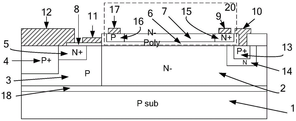
[0033] like figure 1 , as shown in 2, 3, 4, including substrate 1, drift region 2, buried oxygen 18, anode 13, channel region 3, ohmic contact heavily doped region 4, cathode 5, gate 11, gate dielectric 8, Anode lead-out line 10, cathode lead-out line 12, buffer zone 14, drift zone 2, buffer zone 14, and cathode 5 are N-type; substrate 1, channel zone 3, ohmic contact heavily doped zone 4, and anode 13 are P-type ; The electric field strengthening unit 20 provided on the surface of the drift region 2 and the buffer region 14 can also extend to the anode 13 or the channel region 3 . The electric field strengthening unit 20 is isolated from other parts of the transistor by the insulating medium 6 . The electric field strengthening unit 20 includes a high-resistance conductive region 7 , an accelerating gate heavily doped region 15 , a ground doping region 16 , an accelerating gate 9 and a ground electrode 17 . The accelera...

Embodiment 1

[0039] see figure 1 , Figure 8 , Figure 9 . This embodiment uses P- as the substrate (1), uses N- as the drift region (1), P+ as the anode (13), N as the buffer zone (14), P as the channel region (3), and N+ as the cathode (5), P+ acts as an ohmic contact heavily doped region (4). The electric field strengthening unit 20 is arranged on the surface of the drift region 2 and the buffer zone 14, wherein N- or P-polysilicon is used as a high-resistance conductive region (7), N+ polysilicon is used as an accelerated gate heavily doped region (15), and the accelerated gate (9 ) is in direct contact with the heavily doped region (15) of the accelerating gate, and the grounded doped region (16) is doped with a P-type medium concentration.

[0040] When the device is in the cut-off state, the voltage of the anode 13 is high, and the voltage of the grid 11 and cathode 5 is low. At this time, the accelerating grid 9 needs to be set to the same high voltage level as the anode 13, an...

Embodiment 2

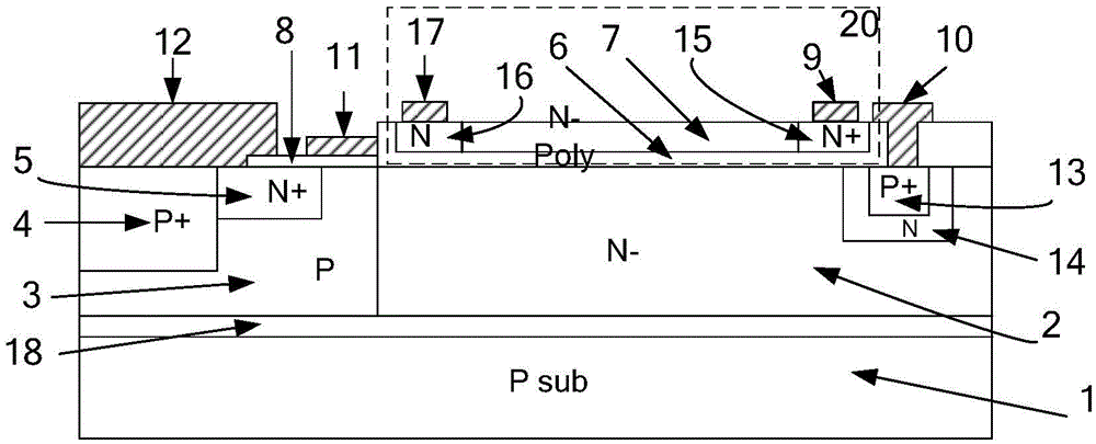
[0044] see figure 2 . This embodiment uses P- as the substrate (1), uses N- as the drift region (1), P+ as the anode (13), N as the buffer zone (14), P as the channel region (3), and N+ as the cathode (5), P+ acts as an ohmic contact heavily doped region (4). The electric field strengthening unit 20 is arranged on the surface of the drift region 2 and the buffer zone 14, wherein the lightly doped N- or P-polysilicon is used as the high-resistance conductive region (7), the accelerated gate heavily doped region (15) and the ground doped region (16) respectively use the same heavily doped and moderately doped polysilicon as the doping type of the high-resistance conductive region (7), and the acceleration grid (9) and the ground electrode (17) are respectively arranged in the high-resistance conductive region (7) Close to both sides of grid (11) and anode (10).

[0045] When the device was in cut-off state, the accelerating grid (9) was set to the same high potential as the ...


PUM


Abstract

Provided is a superspeed heavy current LIGBT, relating to the semiconductor power device. The superspeed heavy current LIGBT comprises a silicon substrate, and a drift region, a channel region, an ohmic contact heavily doped region, a cathode, a grid medium, an anode leading-out wire, a grid, a cathode leading-out wire and an anode which are all arranged above the silicon substrate and buried oxide. The drift region is provided with an electric field strengthening unit on the upper surface of the portion between the anode and the channel region; and the electric field strengthening unit is used for generating an electric field pointing to the lower surface of the electric field strengthening unit from the anode, and is isolated from the drift region through an insulating medium. The superspeed heavy current LIGBT improves the conduction performance and switching performance of an LIGBT device.

Description

technical field [0001] The invention relates to semiconductor power devices, especially the materials and structures of twin conduction power devices. Background technique [0002] It is well known that conventional lateral twin power devices conduct electricity by introducing a large number of holes and electrons through the large injection effect. For example, the most typical lateral insulated gate bipolar transistor device (LIGBT), due to the use of twin conduction, has a small on-resistance, and its on-state voltage drop is much smaller than that of a metal oxide semiconductor device (MOS) under the same conditions. Although MOS devices use multi-sub-conduction, resulting in large on-resistance, their switching speed is extremely fast; however, because LIGBT utilizes twin-sub-conduction, there will be a large number of unbalanced carriers in the drift region when the power device is turned off, and they cannot It is neutralized in a short time, which leads to a long-la...

Claims


Application Information

Patent Timeline
IPC IPC(8): H01L29/739H01L29/06
CPCH01L29/06H01L29/0607H01L29/7393
Inventor 李俊宏李平
Owner UNIV OF ELECTRONIC SCI & TECH OF CHINA
Why Eureka
Try Eureka