Vertical structure light-emitting diode and production method thereof

A light-emitting diode, vertical structure technology, applied in the direction of electrical components, circuits, semiconductor devices, etc., can solve the problem that miniature light-emitting diodes have not been proposed, and achieve the effect of achieving light-emitting effect and improving light-emitting efficiency.

Active Publication Date: 2016-05-18
XIAMEN SANAN OPTOELECTRONICS TECH CO LTD
View PDF10 Cites 5 Cited by
  • Summary
  • Abstract
  • Description
  • Claims
  • Application Information

AI Technical Summary

Problems solved by technology

However, methods and structures for combining micro-LEDs with hexagonal pyramidal structures have not been proposed

Method used


Image

  • Vertical structure light-emitting diode and production method thereof
  • Vertical structure light-emitting diode and production method thereof
  • Vertical structure light-emitting diode and production method thereof

Examples


Embodiment 1

[0029] Such as Figure 1~10 As shown, this embodiment provides a method for fabricating a vertical light-emitting diode, including the following process steps:

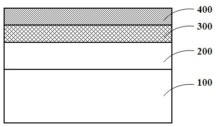
[0030] (1) if figure 1 As shown, a first substrate 100 is provided; in this embodiment, a light-emitting epitaxial layer is grown on the first substrate 100 by MOCVD (metal organic vapor deposition), and the light-emitting epitaxial layer includes a first epitaxial layer 200, a light-emitting layer 300 and a second epitaxial layer in sequence. 400.

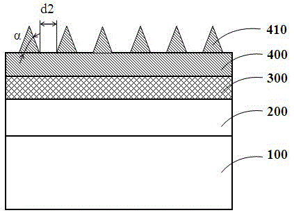
[0031] (2) if Figure 2~3 As shown, a plurality of second hexagonal pyramids 410 are formed on the surface of the second epitaxial layer 400 through an epitaxial process. Specifically, the epitaxial process for forming the second hexagonal pyramids 410 is as follows: using light on the surface of the second epitaxial layer 400 Resist opening mask, the photoresist of this embodiment adopts SU-8 photoresist opening mask, make SU-8 pattern, as etching barrier layer. The...

Embodiment 2

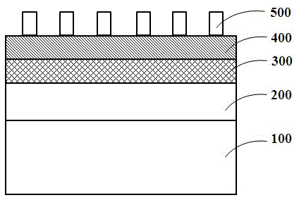
[0039] Such as Figure 7 As shown, the difference between this embodiment and embodiment 1 is that in step (6), the mask layer 500 uses SiO 2 or SiN x With increased etch selectivity, this embodiment is preferably SiO 2 , using the photomask process to fabricate patterned SiO 2 The layer corresponds to the position of the second hexagonal pyramid 410 . Using dry etching technique, etching is carried out in ICP inductively coupled plasma equipment. Carry out the first stage of etching first, etch away the photoresist layer and etch out a certain depth of SiO2 layer and epitaxial layer, the etching gas components used include: CHF 3 and Ar, where CHF 3 The ratio to Ar is 3:1~20:1, the power of ICP is 150W~170W, and the reaction time is 5min~10min. After the photoresist layer is etched, the second stage of etching is performed to etch away the SiO2 layer and the epitaxial layer. The etching gas used is: the etching gas used is Cl 2 and Ar, where Cl 2 The ratio of Ar to Ar...


PUM


Abstract

The invention provides a vertical structure light-emitting diode and a production method thereof. A mini-sized micron or nanometer rod-shaped vertical structure light-emitting diode having two hexagonal cone-shaped end surfaces can be produced by adopting the etching technology and the substrate stripping technology. The requirements of the biomedical field, the photoelectric field, and other fields related to the mini-sized light-emitting diode on the mini-sized light-emitting diode can be satisfied.

Description

technical field [0001] The invention relates to the field of semiconductor optoelectronic devices, in particular to a vertical structure light emitting diode and a manufacturing method thereof. Background technique [0002] In recent years, light-emitting diodes (LEDs) are developing in the direction of high brightness and miniaturization (micron or even nanometer level). The application of micro-LEDs in biomedicine and other fields is developing more and more rapidly. Due to the large difference between the refractive index of GaN-based LEDs and air, there is a problem of low light extraction efficiency. The surface of a GaN-based vertical structure LED usually adopts a patterned hexagonal pyramidal GaN layer structure on one side to improve light extraction efficiency. However, methods and structures for combining micro-LEDs with hexagonal pyramidal structures have not been proposed yet. The market needs to invent a kind of miniature high-brightness vertical structure L...

Claims


Application Information

Patent Timeline
Patent Type & Authority Applications(China)
IPC IPC(8): H01L33/00H01L33/22
CPCH01L33/0075H01L33/22
Inventor 吴政黄邑李佳恩徐宸科
Owner XIAMEN SANAN OPTOELECTRONICS TECH CO LTD
Why Eureka
Try Eureka