

Method for improving copper film thickness consistency during alkaline CMP of GLSI silicon through holes
A technology of copper film thickness and consistency, which is applied to polishing compositions containing abrasives, grinding devices, grinding machine tools, etc., can solve the unmentioned problems of copper film thickness consistency, reduce damaged layers, facilitate removal, The effect of improving uniformity
- Summary
- Abstract
- Description
- Claims
- Application Information
AI Technical Summary
Problems solved by technology
Method used
Image

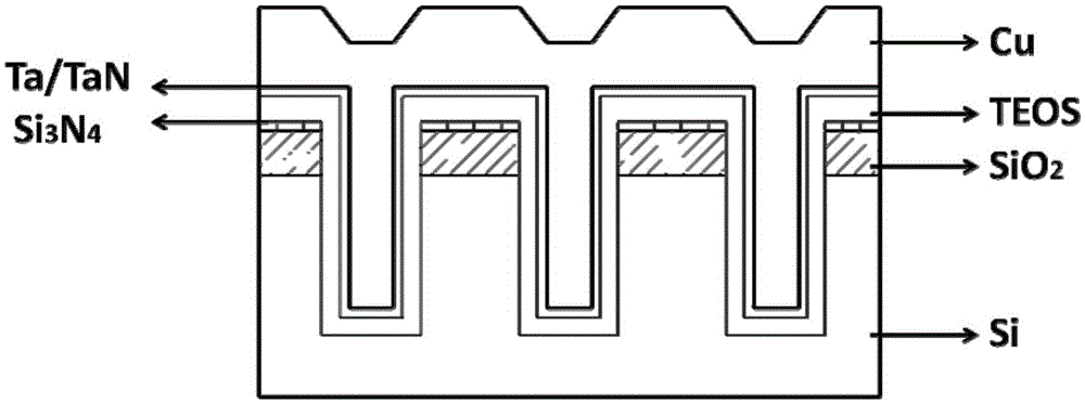
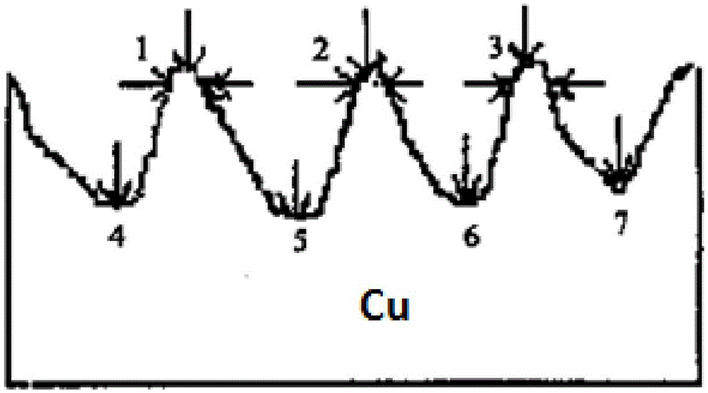
Examples
Embodiment 1
[0028] Prepare 2kgFA / O polishing solution for chemical mechanical polishing.
[0029] Take 1000g of silica hydrosol with a particle size of 80nm, add 50gFA / OⅡtype chelating agent while stirring, then add 15gFA / OⅠtype surfactant while stirring, then add it into 927.5g of deionized water while stirring, and finally Add 7.5g of hydrogen peroxide while stirring; wipe the polishing piece with absolute alcohol, rinse off the residual alcohol with water, and load the polishing piece on the polishing machine table. Working pressure: 27.4kpa; polishing head / disc speed: 65 / 60rpm; flow rate: 225mL / min, polishing time: 180s. After polishing, take out the polishing sheet, first rinse it with water, then dry the water with nitrogen, put the polishing sheet in a dust-free box and send it to the testing room. The results are: the copper film removal rate is 1.94μm / min; the non-uniformity within the chip is 2.9%.
Embodiment 2
[0031] Prepare 2kgFA / O polishing solution for chemical mechanical polishing.
[0032] Take 1000g of silica hydrosol with a particle size of 80nm, add 50gFA / OⅡtype chelating agent while stirring, then add 15gFA / OⅠtype surfactant while stirring, then add it into 927.5g of deionized water while stirring, and finally Add 7.5g of hydrogen peroxide while stirring; wipe the polishing piece with absolute alcohol, rinse off the residual alcohol with water, and load the polishing piece on the polishing machine table. Working pressure: 27.4kpa; polishing head / disk speed: 85 / 80rpm; flow rate: 225mL / min, polishing time: 180s. After polishing, take out the polishing sheet, first rinse it with water, then dry the water with nitrogen, put the polishing sheet in a dust-free box and send it to the testing room. The results are: the copper film removal rate is 1.92μm / min; the non-uniformity within the chip is 3.2%.
Embodiment 3
[0034] Prepare 2kgFA / O polishing solution for chemical mechanical polishing.
[0035]Take 1000g of silica hydrosol with a particle size of 80nm, add 50gFA / OⅡtype chelating agent while stirring, then add 15gFA / OⅠtype surfactant while stirring, then add it into 927.5g of deionized water while stirring, and finally Add 7.5g of hydrogen peroxide while stirring; wipe the polishing piece with absolute alcohol, rinse off the residual alcohol with water, and load the polishing piece on the polishing machine table. Working pressure: 27.4kpa; polishing head / disk speed: 105 / 100rpm; flow rate: 225mL / min, polishing time: 180s. After polishing, take out the polishing sheet, first rinse it with water, then dry the water with nitrogen, put the polishing sheet in a dust-free box and send it to the testing room. The results are: the copper film removal rate is 1.91μm / min; the non-uniformity within the chip is 3.7%.
PUM
| Property | Measurement | Unit |
|---|---|---|
| Particle size | aaaaa | aaaaa |
Abstract
Description
Claims
Application Information