Method of preparing low-dislocation density GaN thin film on Si substrate by adopting carbon nanotubes as periodic dielectric mask

A technology of carbon nanotubes and carbon nanotube arrays, applied in semiconductor/solid-state device manufacturing, electrical components, circuits, etc., can solve problems related to compound polarity, damage to interface flatness, damage to crystal quality, etc.

Active Publication Date: 2016-05-25
SINO NITRIDE SEMICON +1
View PDF3 Cites 10 Cited by
  • Summary
  • Abstract
  • Description
  • Claims
  • Application Information

AI Technical Summary

Problems solved by technology

However, the problems and difficulties in growing GaN on Si substrates by metalorganic vapor phase epitaxy (MOVPE) method lie in: ① The lattice distortion of (0001) GaN wurtzite structure and Si (111) substrate with diamond structure The ratio is 20.4%, which will generate a large number of dislocations; ②The thermal mismatch between GaN and Si is as high as 56%, and the epitaxial layer will bear a large tensile stress during the cooling project after the epitaxial growth is completed
Since the thickness of the epitaxial layer is much smaller than that of the substrate, microcracks will occur in the epitaxial layer, which seriously affects the characteristics of GaN devices
③ When GaN is directly grown on Si substrate, NH 3 I

Method used


Image

  • Method of preparing low-dislocation density GaN thin film on Si substrate by adopting carbon nanotubes as periodic dielectric mask
  • Method of preparing low-dislocation density GaN thin film on Si substrate by adopting carbon nanotubes as periodic dielectric mask
  • Method of preparing low-dislocation density GaN thin film on Si substrate by adopting carbon nanotubes as periodic dielectric mask

Examples


Embodiment 1

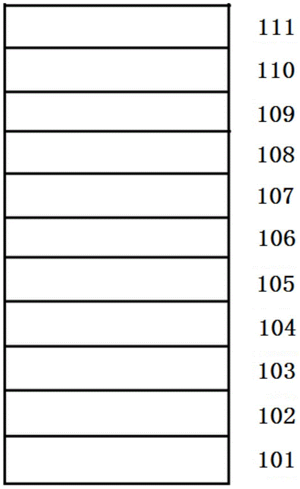
[0032] Use the product of Aixtron Company - tightly coupled vertical reaction chamber MOCVD growth system. During the growth process, trimethylgallium (TMGa) and trimethylaluminum (TMAl) were used as group III sources, ammonia (NH 3 ) as a Group V source, silane (SiH 4 ) as an n-type dopant source, dimagnesocene (Cp 2 Mg) as a p-type dopant source, the Si substrate 101 was first heated to 1080° C. in the MOCVD reaction chamber, and the 2 Under the atmosphere, treat at high temperature for 5-10 minutes. Then in the metal organic compound vapor phase epitaxy reaction chamber, under hydrogen (H 2 ) atmosphere, temperature 1000℃~1500℃, reaction chamber pressure 50torr-100torr, take V / III ratio as 50~1000, feed TMAl as group III source, NH 3 As the V group source, on the Si substrate 101, grow a 0.1 micron thick AlN nucleation layer 102; adopt low-pressure chemical vapor deposition (LPCVD), use acetylene as the carrier gas, use Fe as the catalyst, on the AlN nucleation layer 10...

Embodiment 2

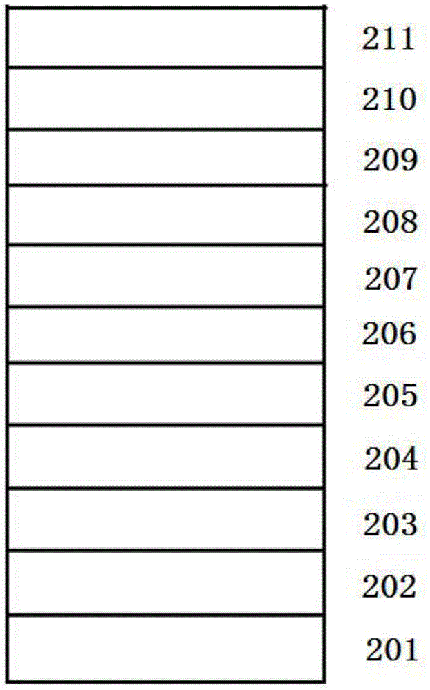
[0034]Use the product of Aixtron Company - tightly coupled vertical reaction chamber MOCVD growth system. During the growth process, trimethylgallium (TMGa) and trimethylaluminum (TMAl) were used as group III sources, ammonia (NH 3 ) as a Group V source, silane (SiH 4 ) as an n-type dopant source, dimagnesocene (Cp 2 Mg) as a p-type dopant source, the Si substrate 201 was first heated to 1080° C. in an MOCVD reaction chamber, and 2 Under the atmosphere, treat at high temperature for 5-10 minutes. Then in the metal organic compound vapor phase epitaxy reaction chamber, under hydrogen (H 2 ) atmosphere, temperature 1000℃~1500℃, reaction chamber pressure 50torr-100torr, take V / III ratio as 50~1000, feed TMAl as group III source, NH 3 As a V group source, on a Si substrate 201, grow a 0.3 micron thick AlN nucleation layer 202; use low-pressure chemical vapor deposition (LPCVD) to grow neatly arranged four-layer unidirectional (crossed) carbon nanotubes. In the growth process,...


PUM

PropertyMeasurementUnit
Diameteraaaaaaaaaa

Abstract

The invention provides a method of preparing a low-dislocation density GaN thin film on a Si substrate by adopting carbon nanotubes as a periodic dielectric mask. The method comprises steps: trimethylgallium (TMGa) and trimethylaluminum (TMAl) are used as an III-group source, an ammonia gas (NH3) serves as a V-group source, silane (SiH4) serves as an n-type doping source, after a high-temperature AlN nucleation layer grows on the Si substrate, two layers or three layers or four layers one-way (crossed) carbon nanotube periodic dielectric masks are prepared to pattern the AlN/Si substrate layer; then, a selective area epitaxial method is adopted to grow a low-Al component AlxGa1-xN merged layer with a thickness of 0.3 to 0.5 micrometer and the Al component no more than 0.25 on the patterned AlN/Si substrate template; then, four layers of GaN grow respectively, three layers of low-temperature AlyGa1-yN stress control layers are inserted in two GaN layers, wherein the Al component y is gradually decreased along with the increasing of layers and y is no less than 0.5 but no more than 1; and thus, the low-dislocation density, non-crack and high-crystal quality GaN/Si thin film can be acquired, wherein the thin film has a thickness of 2 micrometer, the half width of the 002 surface is 500 aresec, and the half width of the 102 surface is 610 aresec.

Description

technical field [0001] The invention belongs to the technical field of semiconductor optoelectronics, and relates to a method for preparing a low dislocation density GaN thin film on a Si substrate, in particular to a method for patterning an AlN / Si substrate template using a carbon nanotube periodic dielectric mask, and forming an AlN / Si substrate template on a GaN During the growth process, the technology of inserting and growing a multilayer low-temperature AlGaN layer whose Al composition decreases with the increase of the layer is used as the stress control layer, and the method of preparing a GaN film with low dislocation density, no cracks and high crystal quality on the Si substrate. Background technique [0002] The Si substrate is large in size and cheap, which can reduce the cost of epitaxial growth. Compared with the insulating sapphire substrate with high hardness and poor thermal conductivity, the conductive Si substrate can effectively simplify the substrate t...

Claims


Application Information

Patent Timeline
IPC IPC(8): H01L21/02
Inventor 贾传宇殷淑仪张国义
Owner SINO NITRIDE SEMICON
Why Eureka
Try Eureka