System-level packaging technology for VGA/YPbPr-to-HDMI interface module

An HDMI interface, system-level packaging technology, applied in electrical components, electrical solid devices, circuits, etc., can solve the problems of low system integration, high cost, unstable signal conduction performance, etc., to shorten the connection path and reduce circulation. , the effect of saving labor costs and material costs

Inactive Publication Date: 2016-05-25
宏晶微电子科技股份有限公司
View PDF3 Cites 1 Cited by
  • Summary
  • Abstract
  • Description
  • Claims
  • Application Information

AI Technical Summary

Problems solved by technology

Using this combination of package forms to realize VGA/YPbPr to HDMI interface module, the system integration is not high, and

Method used


Image

  • System-level packaging technology for VGA/YPbPr-to-HDMI interface module
  • System-level packaging technology for VGA/YPbPr-to-HDMI interface module
  • System-level packaging technology for VGA/YPbPr-to-HDMI interface module

Examples


Embodiment Construction

[0017] In order to make the object, technical solution and advantages of the present invention clearer, the present invention will be further described in detail below in conjunction with the accompanying drawings and embodiments. It should be understood that the specific embodiments described here are only used to explain the present invention, not to limit the present invention.

[0018] VGA / YPbPr of the present invention turns the processing procedure of HDMI interface module system-level packaging technology, and it comprises the following steps:

[0019] S1: Wafer thinning: Mechanical or chemical mechanical grinding is performed from the back of the wafer to thin the wafer to a thickness suitable for packaging;

[0020] S2: Wafer cutting: After the wafer is thinned, it can be diced, and the chip can be cut according to the designed size;

[0021] S3: Chip bonding: Bond the cut chip to the middle pad in the frame. The size of the pad needs to match the chip size;

[002...


PUM


Abstract

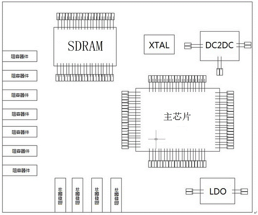
The invention relates to a system-level packaging technology for a VGA/YPbPr-to-HDMI interface module, and aims to reduce the size of the finished VGA/YPbPr-to-HDMI interface module, reinforce signal transmission, improve thermal property and electrical performance, and save cost by adopting the system-level packaging technology. The adopted technical scheme for solving the technical problems is as follows: the system-level packaging technology is adopted; a wire bond technology and SMT patch technology are combined; necessary modules and resistor and capacitor devices in a VGA/YPbPr-to-HDMI interface chip are arranged in a chip to be packaged and moulded in a stacked or tiled manner, so that the overall system function is realized thorough the single chip. The system-level packaging technology has the technical characteristics of capabilities of realizing multi-chip stacking and packaging, passive device packaging, and signal connection in the wire bond and SMT patch connecting ways.

Description

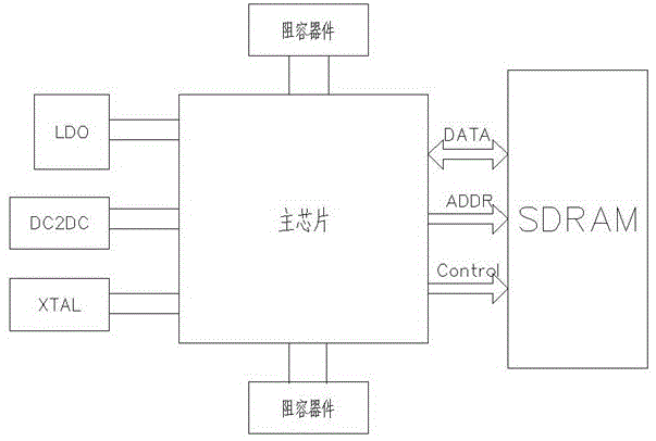
technical field [0001] The present invention relates to semiconductor packaging technology, more specifically, to a system-level packaging technology applicable to a VGA / YPbPr-to-HDMI interface module. Background technique [0002] At present, in order to achieve a better transmission effect, the VGA / YPbPr to HDMI interface module usually needs to be equipped with 1 main control chip, 1 SDRAM as FrameBuffer to transmit data, 1 crystal oscillator as the oscillation circuit, 1 LDO chip and 1 The DC2DC chip is used as a power supply, and several resistive capacitor devices are required as peripheral devices. [0003] Under single-chip packaging technology, a package contains only one die, and the VGA / YPbPr to HDMI module requires multiple functions to be realized. These functions cannot be realized on one die, so multiple dies are required to be packaged separately. A large PCB board is required to realize signal processing between multiple chips. The VGA / YPbPr-to-HDMI interf...

Claims


Application Information

Patent Timeline
IPC IPC(8): H01L25/16H01L25/18
CPCH01L2224/48091H01L2224/48227H01L2224/49175H01L2924/15311H01L2924/19105H01L2924/00014H01L25/16H01L25/18
Inventor 王莉君刘伟刘江
Owner 宏晶微电子科技股份有限公司
Why Eureka
Try Eureka