
Three-dimensional multi-trench gate enhanced HEMT device and preparation method thereof

An enhanced, slot-gate technology, applied in semiconductor/solid-state device manufacturing, semiconductor devices, electrical components, etc., can solve problems such as low effective utilization, low current density, and damage to the continuity of the AlGaN layer, so as to reduce material damage, High current density, which is beneficial to the effect of grid heat dissipation

Active Publication Date: 2016-05-25
UNIV OF ELECTRONIC SCI & TECH OF CHINA
View PDF3 Cites 10 Cited by
  • Summary
  • Abstract
  • Description
  • Claims
  • Application Information

AI Technical Summary

Problems solved by technology

However, this type of device destroys the continuity of the AlGaN layer, and there are problems such as low effective utilization of the active area of ​​the device and low current density.

Method used


Image

  • Three-dimensional multi-trench gate enhanced HEMT device and preparation method thereof
  • Three-dimensional multi-trench gate enhanced HEMT device and preparation method thereof
  • Three-dimensional multi-trench gate enhanced HEMT device and preparation method thereof

Examples


Embodiment Construction

[0033] Embodiments of the present invention are described below through specific examples, and those skilled in the art can easily understand other advantages and effects of the present invention from the content disclosed in this specification. The present invention can also be implemented or applied through other different specific implementation modes, and various modifications or changes can be made to the details in this specification based on different viewpoints and applications without departing from the spirit of the present invention.

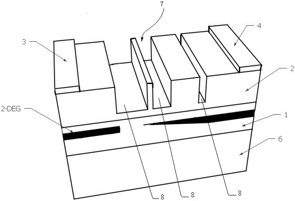
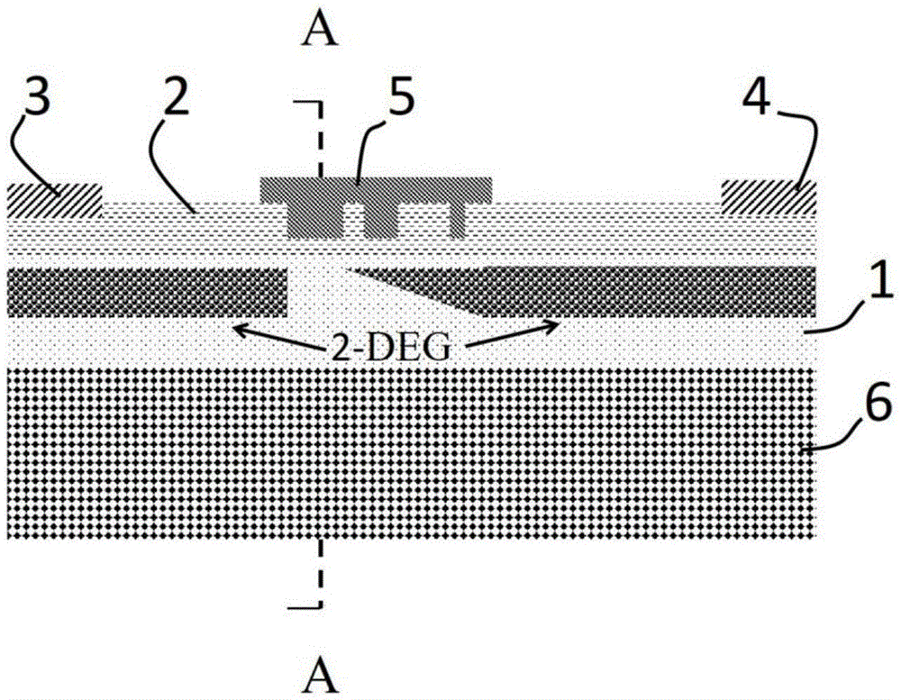
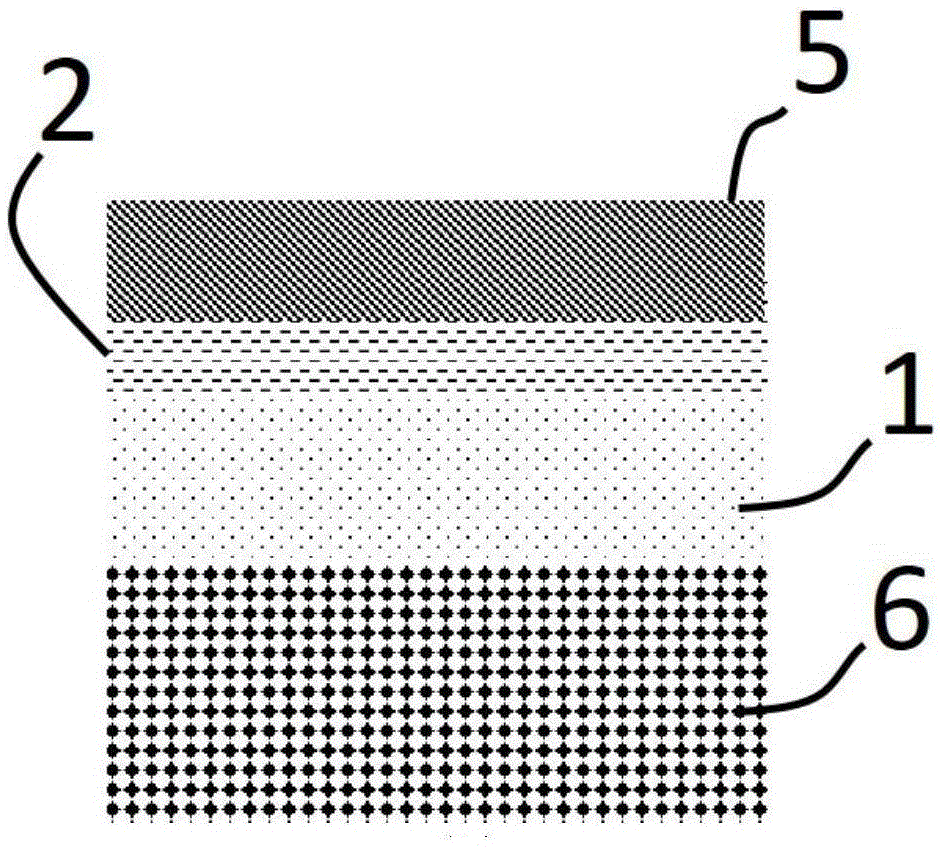
[0034] A three-dimensional multi-groove gate enhanced HEMT device, comprising a substrate 6, a heterojunction above the substrate 6, a gate 5, a source 3 and a drain 4, the heterojunction is composed of a GaN layer 1 and a GaN layer 1 The upper XN2 layer is formed, the gate 5 is located above the heterojunction and forms a Schottky contact with it, the source 3 is located on the surface of the XN layer 2 and forms an ohmic contact with...


PUM


Abstract

The invention provides a three-dimensional multi-trench gate enhanced HEMT device and a preparation method thereof. The three-dimensional multi-trench gate enhanced HEMT device comprises a substrate, a heterojunction, a gate, a source and a drain, wherein the heterojunction is arranged at the upper part of the substrate; the gate is provided with a three-dimensional multi-trench gate structure formed by a plurality of U-shaped grooves; the three-dimensional multi-trench gate structure is formed by etching the heterojunction; the distances between adjacent U-shaped grooves are sequentially reduced in the direction from the drain to the source; and the lengths of the U-shaped grooves are sequentially increased. The preparation method comprises the following steps: manufacturing a wafer of the device; defining isolation between the active region of the device and the device; depositing a metal film in the areas of the source and the drain to obtain the source and the drain of the device; and locally etching a heterojunction layer to prepare the three-dimensional multi-trench gate structure, and depositing the metal film on the upper part of the three-dimensional multi-trench gate to prepare the gate. Compared with a conventional trench gate structure, by the three-dimensional multi-trench gate structure, the electron concentration at the lower part of the gate gradually changes to form gradient distribution; and electric field distribution of the gate area is optimized, so that the reverse withstand voltage of the device and the reliability in a high electric field are improved.

Description

technical field [0001] The invention relates to the field of semiconductor devices, in particular to a three-dimensional multi-groove gate enhanced HEMT device and a preparation method thereof. Background technique [0002] As one of the most popular wide-bandgap semiconductor materials, GaN has the characteristics of large bandgap, direct bandgap, and high electron mobility. It is widely used in power electronics, optoelectronics, and high-frequency electronic devices. In particular, a thin layer of AlGaN is grown on the surface of GaN to form an AlGaN / GaN heterojunction. Under the dual effects of spontaneous polarization and piezoelectric polarization, a high-concentration two-dimensional electron gas (2-DEG) is formed below the AlGaN / GaN heterojunction interface. The electron concentration, mobility, and saturation velocity in this region are large. High electron mobility transistors (HEMTs) based on AlGaN / GaN heterojunctions have excellent performance and have broad ap...

Claims


Application Information

Patent Timeline
IPC IPC(8): H01L29/778H01L21/335
CPCH01L29/66462H01L29/7787H01L29/7788
Inventor 周琦张安邦施媛媛刘丽王泽恒陈万军张波
Owner UNIV OF ELECTRONIC SCI & TECH OF CHINA
Features
  • Generate Ideas
  • Intellectual Property
  • Life Sciences
  • Materials
  • Tech Scout
  • Unparalleled Data Quality
  • Higher Quality Content
  • 60% Fewer Hallucinations
Learn More