PCB with hollow cavity structure and manufacturing method therefor

The technology of a PCB board and a manufacturing method is applied to the PCB board with a cavity structure and its manufacturing field, which can solve problems such as difficulty and reduce transmission loss, and achieve the effects of simple manufacturing process, reduced loss, and low cost

Inactive Publication Date: 2016-06-01
GUANGZHOU FASTPRINT CIRCUIT TECH +2
View PDF3 Cites 3 Cited by
  • Summary
  • Abstract
  • Description
  • Claims
  • Application Information

AI Technical Summary

Problems solved by technology

To meet the needs of high-speed PCB development, Panasonic, NELCO, Isola and other CCL manufacturers have introduced high-speed PCB materials, such as Megtron6 / 7, Meterowave2000, Tachyon and other materials. The Df of these materials has been reduced to 0.003, which can be said to have been reduced to the limit, Dk / Df value is close to PTFE material, it is difficult to reduce transmission loss by improving material performance

Method used


Image

  • PCB with hollow cavity structure and manufacturing method therefor
  • PCB with hollow cavity structure and manufacturing method therefor

Examples


Embodiment Construction

[0023] Below, in conjunction with accompanying drawing and specific embodiment, the present invention is described further:

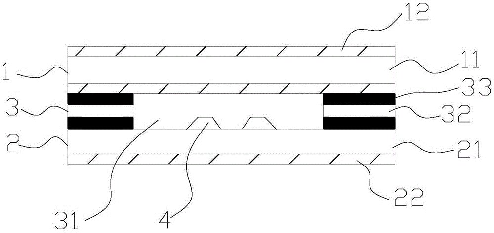
[0024] see figure 1 , the present invention provides a PCB board with a cavity structure, which is a multilayer board, including a first copper clad laminate 1, a second copper clad laminate 2, an adhesive sheet substrate 3 and a differential transmission line 4, the first copper clad laminate 1. The bonding sheet base material 3 and the second copper clad laminate 2 are arranged in sequence from top to bottom. The first copper clad laminate 1 comprises a first light plate 11, the upper end surface and the lower end surface of the first light plate 11 are respectively provided with a first copper clad layer 12; the second copper clad laminate 2 comprises a second light plate 21, the lower surface of the second light plate 21 The end face is provided with the second copper clad layer 22; The upper end surface of the bonding sheet 3 is milled to form a ...


PUM


Abstract

The invention relates to a PCB with a hollow cavity structure and a manufacturing method therefor. The PCB comprises a first copper-coated plate, a second copper-coated plate, a bonding sheet substrate and a differential transmission line, wherein the first copper-coated plate comprises a first optical plate; first copper-coated layers are arranged on the upper end plane and the lower end plane of the first optical plate respectively; the second copper-coated plate comprises a second optical plate; a second copper-coated layer is arranged on the lower end plane of the second optical plate; the upper end plane of the bonding sheet substrate is adhered to the first copper-coated layer on the lower end plane of the first optical plate; the lower end plane of the bonding sheet substrate is adhered to the upper end plane of the second optical plate; a hollow cavity is formed in the bonding sheet substrate; the differential transmission line and the lower end plane of the second optical plate are fixed; and the differential transmission line is positioned in the hollow cavity. According to the PCB and the manufacturing method therefor, the PCB signal transmission property can be effectively realized, and the loss of the transmission line can be greatly lowered; and in addition, the PCB has a simple manufacturing process and low cost.

Description

technical field [0001] The invention relates to the technical field of PCB boards, in particular to a PCB board with a cavity structure and a manufacturing method thereof. Background technique [0002] With the development of technologies such as big data, cloud computing, and the Internet of Things, data transmission continues to develop in the direction of high frequency and high speed. The traditional PCB mainly plays the role of electrical connection in the communication industry, and when the signal transmission rate reaches Gbps or higher, the transmission loss caused by the transmission line on the PCB must be taken into account, especially for long-distance signal transmission systems, such as backplanes. At present, the single-channel signal transmission rate on high-speed PCBs is generally 10Gbps, and some have reached 25Gbps. With the development of 4G and future 5G technologies, the single-channel signal transmission rate on high-speed PCBs needs to reach 40-60Gb...

Claims


Application Information

Patent Timeline
IPC IPC(8): H05K1/02H05K3/46
CPCH05K1/0298H05K3/4697H05K2201/09227
Inventor 王红飞陈蓓邱醒亚
Owner GUANGZHOU FASTPRINT CIRCUIT TECH
Why Eureka
Try Eureka