Forming method of semiconductor structure

A semiconductor and isolation structure technology, applied in the field of semiconductor structure formation, can solve the problems of semiconductor device electrical performance degradation, etc., achieve the effect of improving formation quality, improving electrical performance, and avoiding voids

Inactive Publication Date: 2016-06-08
SHANGHAI HUAHONG GRACE SEMICON MFG CORP
View PDF4 Cites 26 Cited by
  • Summary
  • Abstract
  • Description
  • Claims
  • Application Information

AI Technical Summary

Problems solved by technology

[0004] However, the shallow trench isolation structure of the prior art is likely to cause the reduction of the electrical performance of the semiconductor device

Method used


Image

  • Forming method of semiconductor structure
  • Forming method of semiconductor structure
  • Forming method of semiconductor structure

Examples


Embodiment Construction

[0021] It can be seen from the background art that the shallow trench isolation structure in the prior art tends to degrade the electrical performance of the semiconductor device. Analyze the reasons for this:

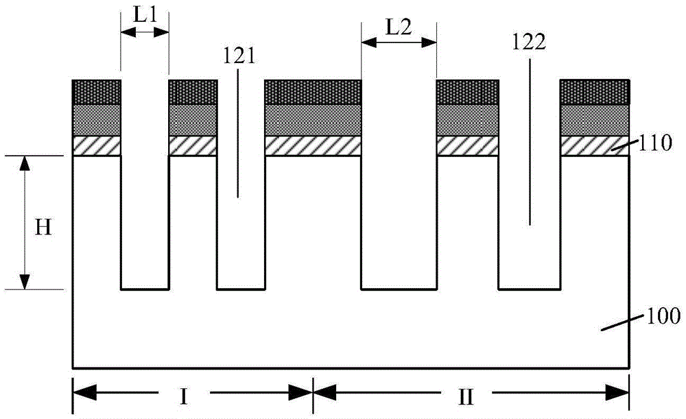
[0022] Such as figure 1 As shown, the substrate 100 of the conventional flash memory includes a core area I and a peripheral area II, the core area I is used to form devices with smaller feature sizes, and the peripheral area II is used to form devices with larger feature sizes. Among them, the distance between the gate electrode layers 110 of adjacent devices in the core region I is small, while the distance between the gate electrode layers 110 of adjacent devices in the peripheral region II is relatively large, that is to say, the two adjacent gate electrodes in the core region I The line width L1 of the shallow trench 121 between the electrode layers 110 is smaller than the line width L2 of the shallow trench 122 between two adjacent gate electrode layers 110 in t...


PUM


Abstract

The invention discloses a forming method of a semiconductor structure. The method comprises the following steps: providing a substrate which comprises a first region for forming a core storage circuit; orderly forming a gate electrode film and an initial hard mask film on the substrate; etching the initial hard mask film by using the first etching process, forming a first opening penetrating through the initial hard mask film in the first region; filling a sacrifice layer in the first opening; etching the sacrifice layer and the substrate at the bottom of the first opening by using the second etching process, and forming a first groove in the first region substrate; and forming a first isolation structure in the first groove. The method comprises: firstly forming the first opening penetrating through the initial hard mask film in the first region, and then filling the sacrifice layer in the first opening to form the first groove, wherien the sacrifice layer is firstly etched along the first opening and then the substrate is etched, thereby acquiring the first groove with small depth so as to reduce the depth-to-width ratio of the first groove; and the condition of forming a gap in the first isolation structure is avoided, thereby improving the forming quality of the first isolation structure, and then improving the electric property of a semiconductor device.

Description

technical field [0001] The invention relates to the field of semiconductors, in particular to a method for forming a semiconductor structure. Background technique [0002] With the development trend of high-density integrated circuits, the devices that make up the circuit are placed more closely in the chip to fit the available space of the chip. Correspondingly, the density of active devices per unit area of ​​the semiconductor substrate continues to increase, so effective insulation between devices becomes more important. [0003] Shallow trench isolation (Shallow Trench Isolation, STI) technology has a good isolation effect (for example: process isolation effect and electrical isolation effect), shallow trench isolation technology also has the advantages of reducing the area occupied by the wafer surface and increasing the integration of devices . Therefore, with the reduction of the size of integrated circuits, the isolation between devices is now mainly using shallow ...

Claims


Application Information

Patent Timeline
Patent Type & Authority Applications(China)
IPC IPC(8): H01L21/762
CPCH01L21/76229H01L21/76224
Inventor 沈思杰张怡
Owner SHANGHAI HUAHONG GRACE SEMICON MFG CORP
Why Eureka
Try Eureka