Three-dimensional stackable phase change storage array device and preparation method thereof

A phase-change storage, three-dimensional stacking technology, applied in semiconductor/solid-state device manufacturing, electrical solid-state devices, semiconductor devices, etc., can solve the problems of high manufacturing cost of three-dimensional PCRAM structure, low reliability of high-density storage architecture, etc., to improve storage Density, reduce process cost, solve the effect of high density

Active Publication Date: 2016-06-08
SHANGHAI INST OF MICROSYSTEM & INFORMATION TECH CHINESE ACAD OF SCI
View PDF4 Cites 9 Cited by
  • Summary
  • Abstract
  • Description
  • Claims
  • Application Information

AI Technical Summary

Problems solved by technology

[0008] In view of the above-mentioned shortcomings of the prior art, the purpose of the present invention is to provide a three-dimensional stacked phase-change memory array device and its preparation method, which is used to solve the problem of high manufacturing cost of the three-dimensional PCRAM structure and reliable high-density storage architecture in the prior art. low sex problem

Method used


Image

  • Three-dimensional stackable phase change storage array device and preparation method thereof
  • Three-dimensional stackable phase change storage array device and preparation method thereof
  • Three-dimensional stackable phase change storage array device and preparation method thereof

Examples


Embodiment 1

[0099] The invention provides a method for preparing a three-dimensional stacked phase-change memory array device, comprising the following steps:

[0100] Step S1 : providing a driving array; the driving array includes a plurality of discrete driving units, and the tops of the driving units are connected with first conductive pillars.

[0101] Specifically, the driving unit includes at least one of a diode, a field effect transistor and a bipolar transistor.

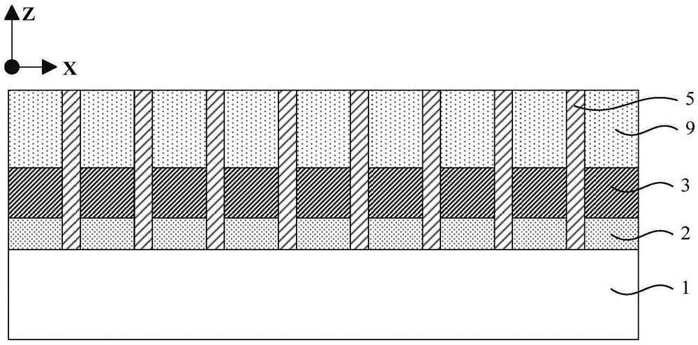
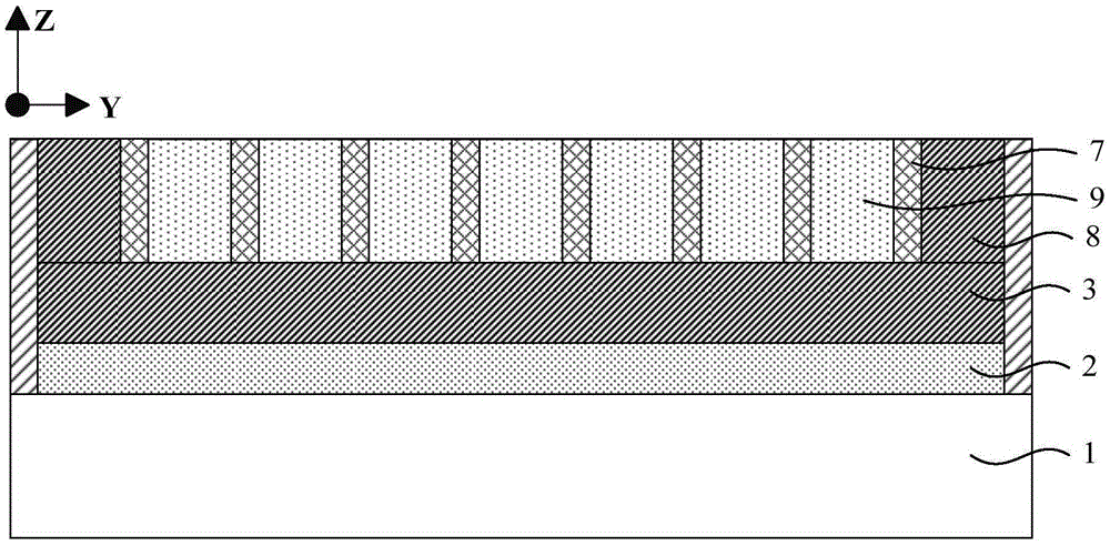
[0102] In this embodiment, the driving unit preferably adopts a diode. As an example, an X-Y-Z coordinate axis is established, wherein the X axis is parallel to the bit line direction, the Y axis is parallel to the word line direction, and the Z axis is perpendicular to the X-Y plane. see Figure 1-Figure 3 , which is a schematic diagram of a driving array. In this embodiment, the driving array preferably adopts a double shallow trench isolation epitaxial diode array structure, wherein, figure 1 It is shown as a sche...

Embodiment 2

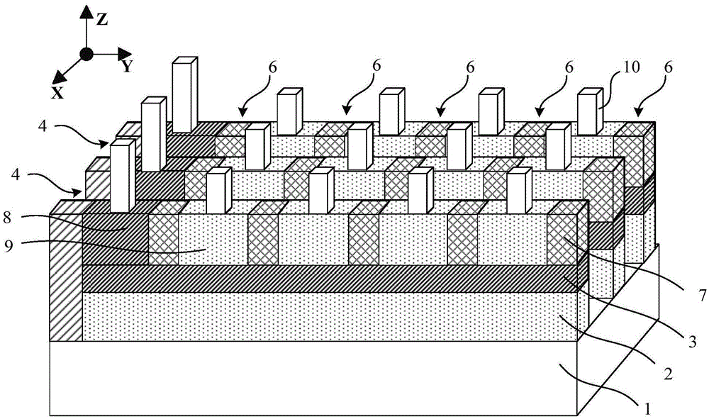
[0140] The present invention also provides a three-dimensional stacked phase-change memory array device, please refer to Figure 10-Figure 12 ,in, Figure 12 It is shown as a perspective view of the three-dimensional stacked phase-change memory array device, Figure 10 shown as Figure 12 The Y-Z plane sectional view of the partial area of ​​the structure shown, Figure 11 shown as Figure 12 The Z-Z plane sectional view of the partial region of the structure shown, as shown in the figure, the three-dimensional stacked phase-change memory array device includes:

[0141] A drive array; the drive array includes a number of discrete drive units, the top of which is connected to a first conductive column 10;

[0142] A plurality of multi-layer grid strip structures formed above the driving array and parallel to the direction of the word lines; the multi-layer grid strip structure includes at least two layers of gate material layers 11, and the adjacent two layers of gate mater...


PUM


Abstract

The invention provides a three-dimensional stackable phase change storage array device and a preparation method thereof. In the three-dimensional stackable phase change storage array device, a grid electrode of a non-junction type transistor adopts a stepped elicitation mode of a control grid electrode to form an SSL control end. A phase change storage unit exists at the junction point of a WL, a BL and the SSL to realize reading, writing and scraping operation on every storage location point. In addition, a stacked structure composed of a grid electrode conductive material and an insulating medium layer stretches across two adjacent wolfram plugs, the sharing of a phase change material layer is realized, the process cost is reduced to a large extent, and the storage density is improved. The preparation method of the three-dimensional stackable phase change storage array device is compatible with a traditional CMOS process, both the formation of the non-junction type transistor and the phase change unit are low temperature process, the heat treatment process has no performance drifting influence on a peripheral circuit, a channel of the non-junction type transistor adopts a heavily doped polycrystalline silicon material without a concentration gradient, and an additional photomask induced by doping processes such as ion injection is effectively avoided.

Description

technical field [0001] The invention belongs to the field of integrated circuit manufacturing, and relates to a three-dimensional stacked phase-change memory array device and a preparation method thereof. Background technique [0002] Semiconductor storage technology is a constantly updated and progressive technology. Developing new semiconductor storage technology and designing high-density storage architecture are effective ways to solve the shortcomings of existing storage products. With the gradual reduction of semiconductor process nodes, the device size will reach its physical limit, which is challenging for high-density mass storage. Therefore, device designers have started research and development of three-dimensional stackable memory structures to meet the requirements of higher storage capacity per storage bit, high reliability, low process cost, and compatibility with CMOS processes. [0003] As claimed by the famous semiconductor company IBM, phase-change rando...

Claims


Application Information

Patent Timeline
Patent Type & Authority Applications(China)
IPC IPC(8): H01L27/24H01L29/167H01L29/423H01L21/82
CPCH01L29/167H01L29/4232H01L21/82H10B63/32H10B63/20H10B63/30
Inventor 刘燕宋志棠宋三年刘波
Owner SHANGHAI INST OF MICROSYSTEM & INFORMATION TECH CHINESE ACAD OF SCI
Why Eureka
Try Eureka