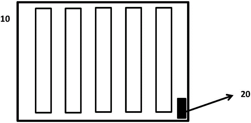
Solar cell with high-sensitivity humidity detector
A humidity detection device and a technology for solar cells, applied in the field of solar cells, can solve problems such as property loss, corrosion, and lack of humidity-sensitive detection function, and achieve the effects of promoting adsorption, simple production process, and increasing humidity-sensitive performance.
- Summary
- Abstract
- Description
- Claims
- Application Information
AI Technical Summary
Problems solved by technology
Method used
Image
Examples
Embodiment 1
[0039] A solar cell with a high-sensitivity humidity detection device. A humidity sensor module is installed on the outside of the solar cell. The humidity sensor module includes heavily doped silicon wafers that are arranged sequentially from bottom to top, and are close to the heavily doped silicon wafers. SiO 2 layer, carbon nanotube layer, on SiO 2 The lower electrode between the layers and the upper electrode on the carbon nanotube layer grown on SiO 2 layer; there is a metal film on the lower electrode, and the metal film is an adhesive Cr layer, a conductive and thermally conductive Cu layer, and an Au layer as an electrode layer from the inside to the outside, and the Cr layer, Cu layer and The thickness of the Au layer is 70nm, 250nm and 500nm in sequence; the carbon nanotube layer adopts catalyst and / or photolithography to achieve its localized growth, and the grown carbon nanotube layer adopts plasma to make it produce hydroxyl modification, The carbon nanotube la...
Embodiment 2
[0058] A solar cell with a highly sensitive humidity detection device, the solar cell is equipped with a humidity sensor module on the outside, the humidity sensor module includes heavily doped silicon wafers arranged in sequence from bottom to top, close to the heavily doped SiO 2 layer, carbon nanotube layer, on SiO 2 The lower electrode between the layers and the upper electrode on the carbon nanotube layer grown on SiO 2 layer; there is a metal film on the lower electrode, and the metal film is an adhesive Cr layer, a conductive and thermally conductive Cu layer, and an Au layer as an electrode layer from the inside to the outside, and the Cr layer, Cu layer and The thickness of the Au layer is 25nm, 125nm and 500nm in sequence; the carbon nanotube layer adopts catalyst and / or photolithography to achieve its localized growth, and the grown carbon nanotube layer adopts plasma to make it produce hydroxyl modification, The carbon nanotube layer has been treated with a mixed...
Embodiment 3
[0077] A solar cell with a high-sensitivity humidity detection device. A humidity sensor module is installed on the outside of the solar cell. The humidity sensor module includes heavily doped silicon wafers that are arranged sequentially from bottom to top, and are close to the heavily doped silicon wafers. SiO 2 layer, carbon nanotube layer, on SiO 2 The lower electrode between the layers and the upper electrode on the carbon nanotube layer grown on SiO 2 layer; there is a metal film on the lower electrode, and the metal film is an adhesive Cr layer, a conductive and thermally conductive Cu layer, and an Au layer as an electrode layer from the inside to the outside, and the Cr layer, Cu layer and The thickness of the Au layer is 35nm, 160nm and 400nm in sequence; the carbon nanotube layer adopts catalyst and / or photolithography to achieve its localized growth, and the grown carbon nanotube layer adopts plasma to make it produce hydroxyl modification, The carbon nanotube la...
PUM
| Property | Measurement | Unit |
|---|---|---|
| thickness | aaaaa | aaaaa |
| thickness | aaaaa | aaaaa |
| thickness | aaaaa | aaaaa |
Abstract
Description
Claims
Application Information

