Image sensor and forming method thereof

An image sensor and pixel area technology, applied in the direction of electric solid-state devices, semiconductor devices, electrical components, etc., can solve the problems of poor performance of image sensors, affect image quality, and generate dark current, so as to reduce the probability of diffusion and dark current , the effect of improving quality

Active Publication Date: 2016-06-15
SHANGHAI HUAHONG GRACE SEMICON MFG CORP
View PDF4 Cites 1 Cited by
  • Summary
  • Abstract
  • Description
  • Claims
  • Application Information

AI Technical Summary

Problems solved by technology

Metal impurities in the top substrate are easily diffused into the semiconductor device in the pixel area during heat treatment, and are trapped to form metal impurity energy levels, resulting in dark current and affecting image quality
[0006] It can be seen that the CIS formed by the silicon-on-insulator substrate in the prior art has the disadvantages of large dark current and poor image sensor performance.

Method used


Image

  • Image sensor and forming method thereof
  • Image sensor and forming method thereof
  • Image sensor and forming method thereof

Examples


Embodiment Construction

[0035] Existing silicon-on-insulator (SOI) CMOS image sensors have problems of large dark current and poor performance.

[0036] Now in combination with a CMOS image sensor, the reasons for the large dark current and poor performance of the silicon-on-insulator (SOI) CMOS image sensor are analyzed:

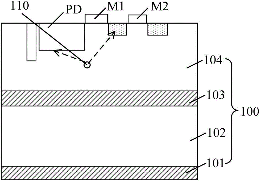
[0037] figure 1 It is a structural schematic diagram of a silicon-on-insulator (SOI) CMOS image sensor. The CMOS image sensor includes:

[0038] SOI substrate 100, described SOI substrate 100 comprises: wafer back absorption layer 101; The underlying substrate 102 that is positioned at the back surface absorption layer 101; The buried oxide layer 103 that is positioned at the bottom substrate 102 surface; The top substrate 104.

[0039] In the pixel area located in the top substrate 104, the pixel area includes a semiconductor device unit, and the semiconductor device unit includes a photodiode PD, a transfer transistor M1 and a reset transistor M2.

[0040] During the process...


PUM


Abstract

The invention provides an image sensor and a forming method thereof. The image sensor comprises a silicon-on-insulator (SOI) substrate, wherein the SOI substrate comprises a wafer back absorption layer, a bottom layer substrate, a buried oxide layer and a top layer substrate; the buried oxide layer is located at the upper part of the bottom layer substrate; the top layer substrate is located at the upper part of the buried oxide layer and comprises a pixel region and an absorption region; the absorption region is located on the periphery of the pixel region; the pixel region comprises a photoelectric diode PD and a transistor unit; an absorption structure is arranged in the absorption region and comprises polycrystal layers and covering layers; the covering layers ares located on the surfaces of the polycrystal layers; and the absorption layer is in a laminated structure which is formed by alternate arrangement of the polycrystal layers and the covering layers; the covering layers are used for inhibiting recrystallization of the polycrystal layers; and the absorption structure can effectively absorb metal impurities in the top layer substrate, reduces the dark current and improves the image quality.

Description

technical field [0001] The invention relates to the technical field of semiconductor manufacturing, in particular to an image sensor and a forming method thereof. Background technique [0002] Image sensors are devices that convert light signals into electrical signals, and are widely used in digital TV and visual communication markets. [0003] CMOS Image Sensors (CMOS Image Sensors, CIS) is an image sensing element manufactured using the principle of photoelectric technology. The composition of its photosensitive pixels is an array structure, which is mainly composed of MOS capacitors or p-n junction photosensitive diodes. CIS is formed by integrating light-sensitive light unit array (photodiode), transfer transistor, reset transistor, source follower transistor and selection transistor on a silicon chip board by traditional chip technology. [0004] Manufacturing a CMOS image sensor by using a silicon-on-insulator (Silicon-On-Insulator, SOI) substrate can effectively re...

Claims


Application Information

Patent Timeline
Patent Type & Authority Applications(China)
IPC IPC(8): H01L27/146
CPCH01L27/1462H01L27/14643H01L27/14685
Inventor 饶金华
Owner SHANGHAI HUAHONG GRACE SEMICON MFG CORP
Why Eureka
Try Eureka