Planar waveguide type near-and-mid infrared light modulator based on graphene-chalcogenide glass

A technology of chalcogenide glass and planar waveguide, applied in the direction of optical waveguide light guide, light guide, optics, etc., can solve the problems of difficult modulation and demodulation of integrated photonic devices, research lag, etc., and achieve small size, high modulation rate, and high extinction ratio Effect

Inactive Publication Date: 2016-06-22
UNIV OF ELECTRONICS SCI & TECH OF CHINA
View PDF5 Cites 17 Cited by
  • Summary
  • Abstract
  • Description
  • Claims
  • Application Information

AI Technical Summary

Problems solved by technology

But at present, generally speaking, the research on optical devices based on mid-infrared, including mid-infrared optical modulators, is still lagging behind, especially the problem of modulation and demodulation of integrated photonic devices based on optical signals of 1.55-3 μm near-mid-infrared

Method used


Image

  • Planar waveguide type near-and-mid infrared light modulator based on graphene-chalcogenide glass
  • Planar waveguide type near-and-mid infrared light modulator based on graphene-chalcogenide glass
  • Planar waveguide type near-and-mid infrared light modulator based on graphene-chalcogenide glass

Examples


Embodiment 1

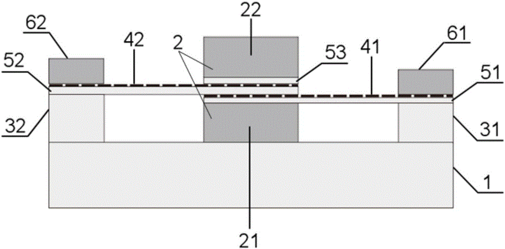
[0038] Schematic diagram of the three-dimensional structure of the near-mid-infrared optical modulator based on graphene-chalcogenide glass planar waveguide. figure 1 As shown: using 1.55-3 μm near-mid-infrared light wavelength, including a base layer 1, a ridge-shaped optical waveguide layer 2 disposed on the base layer 1, a first pillar 31 and a second pillar 32, and the first pillar 31 and the second pillar 32 are arranged on the left and right sides of the ridge-shaped optical waveguide layer 2, and the ridge-shaped optical waveguide layer 2 is divided into a first ridge-shaped optical waveguide layer 21 and a second ridge-shaped optical waveguide layer arranged on the first ridge-shaped optical waveguide layer 21 The waveguide layer 22, the first graphene layer 41 and the second graphene layer 42 are sequentially arranged between the first ridge optical waveguide layer 21 and the second ridge optical waveguide layer 22 from bottom to top; the first graphene The layer 41 e...

Embodiment 2

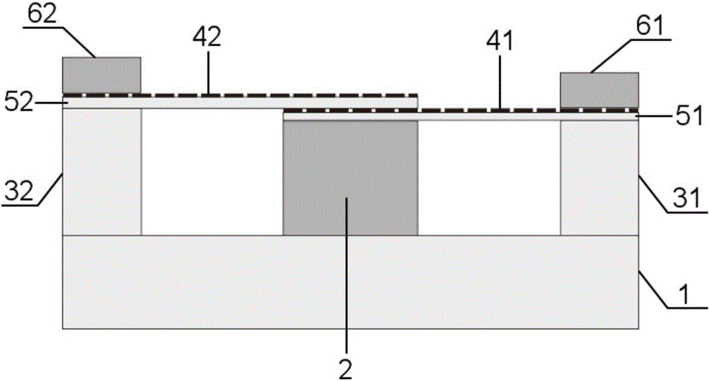
[0040] Schematic diagram of the three-dimensional structure of the near-mid-infrared optical modulator based on graphene-chalcogenide glass planar waveguide. figure 2 As shown: using 1.55-3 μm near-mid-infrared light wavelength, including a base layer 1, a ridge-shaped optical waveguide layer 2 disposed on the base layer 1, a first pillar 31 and a second pillar 32, and the first pillar 31 and the second pillar 32 are arranged on the left and right sides of the ridge-shaped optical waveguide layer 2, and the first graphene layer 41 and the second graphene layer 42 are sequentially arranged on the upper surface of the ridge-shaped optical waveguide layer 2 from bottom to top; the first graphene layer The layer 41 extends to the upper surface of the first pillar 31, and the second graphene layer 42 extends to the upper surface of the second pillar 32. The ridge-shaped optical waveguide layer 2 and the first graphene layer 41, the first graphene layer 41 A first isolation dielect...


PUM

PropertyMeasurementUnit
thicknessaaaaaaaaaa
thicknessaaaaaaaaaa

Abstract

The invention discloses a planar waveguide type near-and-mid infrared light modulator based on graphene-chalcogenide glass, and belongs to the technical field of electro-optical modulators. The optical modulator solves the problems in modulation and demodulation of integrated photonic devices based on optical signals of near-and-mid infrared light ranging from 1.55 microns to 3 microns. The modulator comprises a substrate layer, ridge-shaped light waveguide layers, a first strut and a second strut, wherein the ridge-shaped light waveguide layers, the first strut and the second strut are arranged on the substrate layer; a first graphene layer and a second graphene layer are arranged on the ridge-shaped light waveguide layers; the first graphene layer extends to the upper surface of the first strut, and the second graphene layer extends to the upper surface of the second strut; isolation medium layers are arranged between the ridge-shaped optical waveguide layer and the first graphene layer, between the ridge-shaped optical waveguide layer and the second graphene layer, between the first graphene layer and the second graphene layer, between the first graphene layer and the first strut, and between the second graphene layer and the second strut respectively; a first electrode is arranged on the first graphene layer on the first strut, and a second electrode is arranged on the second graphene layer on the second strut. The modulator is used for signal modulation and demodulation in the integrated photonic devices.

Description

technical field [0001] A near-mid-infrared optical modulator based on graphene-chalcogenide glass planar waveguide, used for integrated photonic devices to modulate and demodulate 1.55-3μm near-mid-infrared optical signals, belonging to electro-optic modulators, especially related to graphene-sulfur based The invention relates to the technical field of glass planar waveguide near-mid infrared light modulators. Background technique [0002] It is an inevitable trend of historical development that photons replace electrons as the carrier of information. The research of modern integrated optics mainly focuses on the near-infrared communication band. With practical application, the wavelength band of integrated optics research has gradually shifted from the first-generation 0.85μm to the second-generation 1.31μm and to the most mainstream 1.555μm wavelength. Various optical devices, including optical waveguides, optical couplers, optical switches, optical modulators, filters, a...

Claims


Application Information

Patent Timeline
Patent Type & Authority Applications(China)
IPC IPC(8): G02F1/035G02B6/12
CPCG02F1/035G02B6/12G02B2006/12038G02B2006/12142
Inventor 陆荣国叶胜威田朝辉刘天良陈德军张尚剑刘永
Owner UNIV OF ELECTRONICS SCI & TECH OF CHINA
Why Eureka
Try Eureka