High selectivity balanced filter based on signal interference technology
A balanced filter, high selectivity technology, applied in the direction of waveguide devices, circuits, electrical components, etc., can solve the problems of increasing filter volume, large volume, complex circuits, etc.
- Summary
- Abstract
- Description
- Claims
- Application Information
AI Technical Summary
Problems solved by technology
Method used
Image
Examples
Embodiment 1
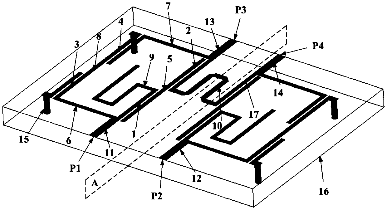
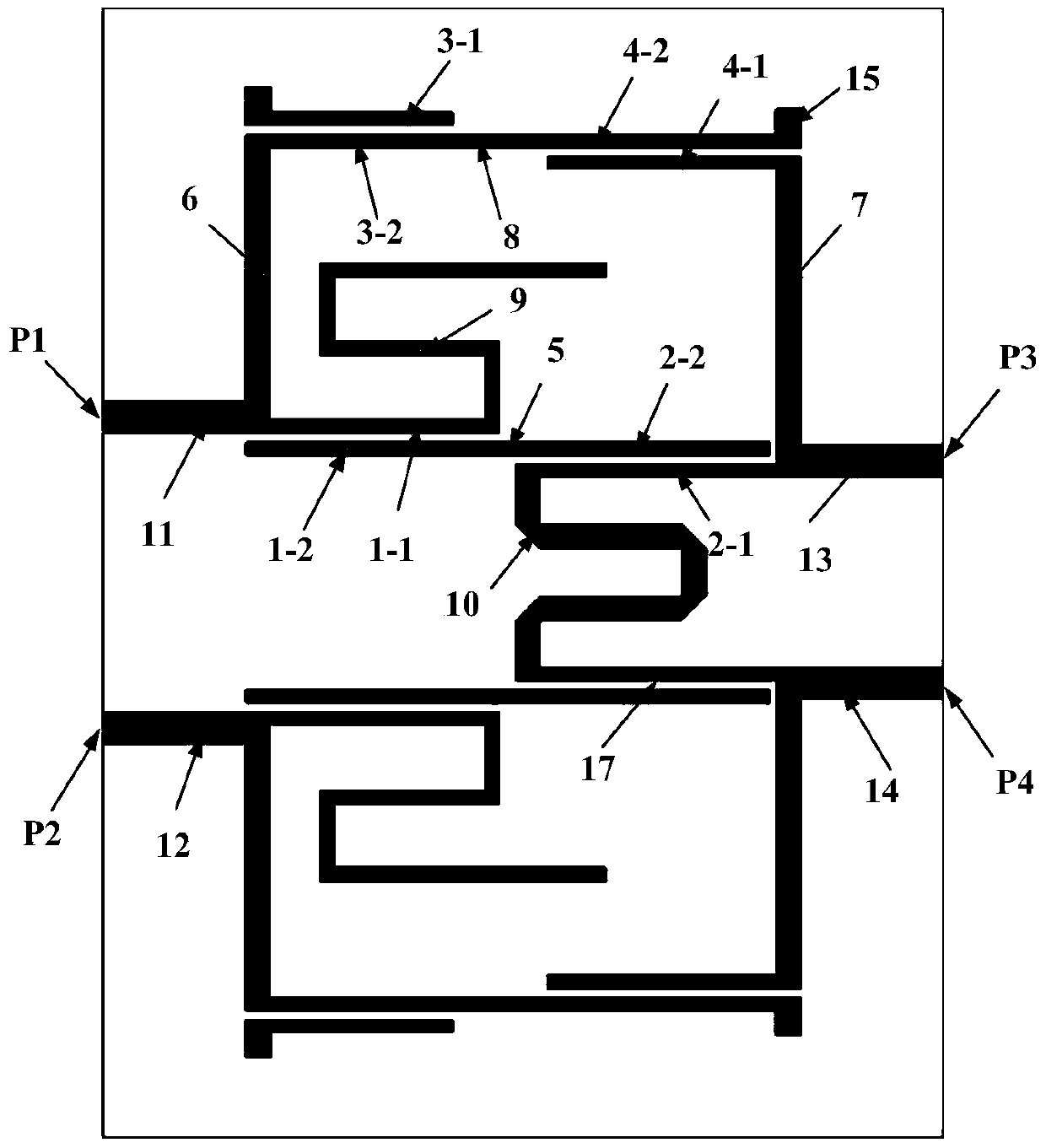
[0026] Since the above-mentioned highly selective balanced filter circuit model is a left-right symmetrical circuit structure, it can be easily analyzed using the difference / common mode theory. For the middle "several" shape transmission line, the differential mode excitation shows a short-circuit characteristic, and the even-mode excitation shows an open-circuit characteristic. According to the balanced filter differential mode circuit model, there are two different transmission paths from port P1 to port P3 (the odd / even mode characteristic impedance of the open coupled line is Z oo1 and Z oe1 , the odd / even mode characteristic impedance of the open / short coupled line is Z oo2 and Z oe2 ), two pairs of open / short coupled lines and the connected two transmission lines form transmission path 1; two pairs of open coupled lines and one loaded short line and one open line form transmission path 2.
[0027] With the coupling coefficient k between the open coupled lines 1 (k 1...
Embodiment 2
[0033] A high-selectivity balanced filter based on signal interference technology, the balanced filter has a left-right symmetrical structure as a whole, and is symmetrical about the center plane A, wherein the first port P1, the second port P2, the third port P3, and the fourth port P4 They are all located on the upper layer of the dielectric substrate. Four 50-ohm microstrip lines are respectively connected to the corresponding four ports. The four 50-ohm microstrip lines are respectively the first microstrip line 11, the second microstrip line 12, and the third microstrip line. The strip line 13 and the fourth microstrip line 14; wherein the first port P1 and the second port P2 are located on one side of the dielectric substrate, the third port P3 and the fourth port P4 are located on the other side of the symmetry of the dielectric substrate, and the first port P1 and the second port P2 are symmetrical about the central plane A, and the third port P3 and the fourth port P4 ...
PUM
 Abstract
Description
Claims
Application Information


