
Semiconductor device manufacturing method

A manufacturing method and semiconductor technology, applied in the manufacture of microstructure devices, techniques for producing decorative surface effects, decorative art, etc., can solve the problems of easy gold residue in the gold layer and low uniformity of the undercut of the gold pattern block, etc. , to achieve the effect of avoiding gold residue

Active Publication Date: 2016-06-29
SEMICON MFG INT (SHANGHAI) CORP
View PDF5 Cites 2 Cited by
  • Summary
  • Abstract
  • Description
  • Claims
  • Application Information

AI Technical Summary

Problems solved by technology

[0005] The problem solved by the invention is that the etching of the existing gold layer is prone to gold residue, and the uniformity of the undercut amount of multiple gold pattern blocks is not high

Method used


Image

  • Semiconductor device manufacturing method
  • Semiconductor device manufacturing method
  • Semiconductor device manufacturing method

Examples


Embodiment Construction

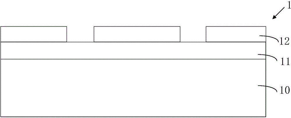
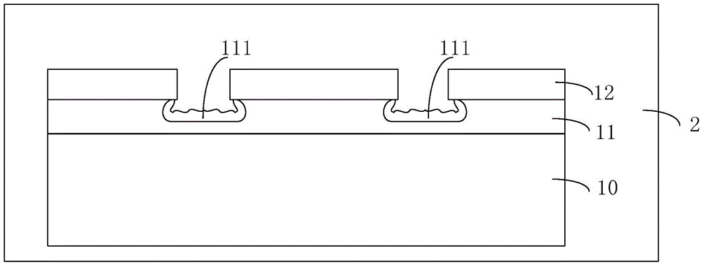
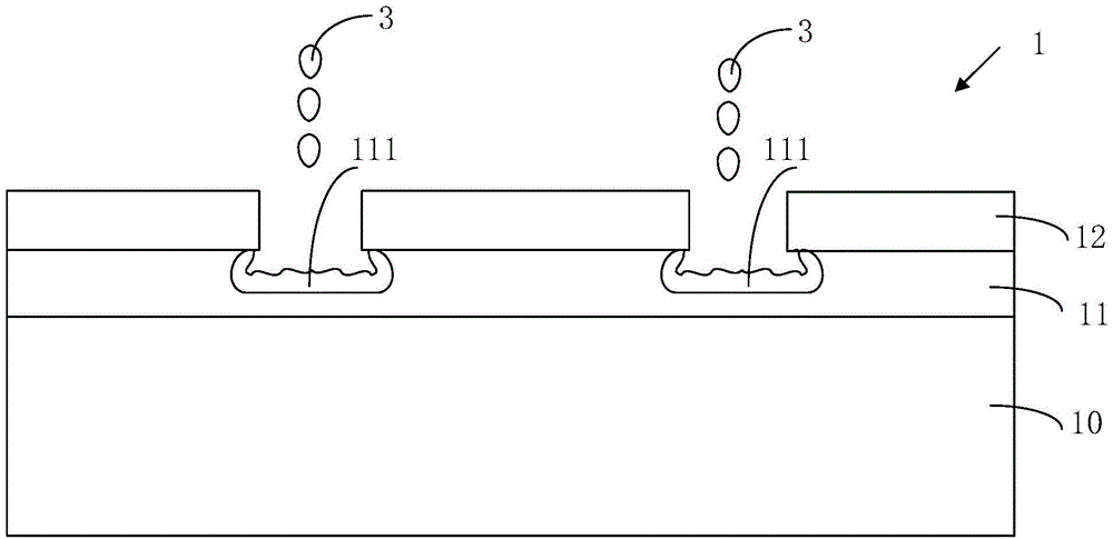
[0024] As mentioned in the background art, there are some problems in the existing etching process of the gold layer. First, gold residue is prone to occur; second, the undercut amount is not uniform, that is, multiple etchings formed in the same batch The horizontal removal of gold pattern blocks varies, some are more, some are less. In view of the above-mentioned problems, the inventors have analyzed and found that the cause of the problem is: if the gold layer is corroded for a long time, for example, using KI and I 2 The above corrosion is isotropic corrosion. It will be found that as time goes by, more and more etching by-products accumulate on the surface of the gold layer. As the gold layer is covered by the etching by-products, it affects the gold The further corrosion rate of the layer and the amount of etching by-products coated in different areas are different. The gold layer in some areas may not be in contact with the etching solution. Therefore, on the one hand, it...


PUM

PropertyMeasurementUnit
Thicknessaaaaaaaaaa

Abstract

A semiconductor device manufacturing method is as follows: a gold layer is patterned by multi-times of wet etching, a wet etching solution is an aqueous solution comprising KI and I2, the time of each time of wet etching is less than 2 minutes, and after each time of wet etching, deionized water is used for rinsing, so that byproducts produced in each time of wet etching can be peeled off in time, further etching rate slow down of the gold layer caused by coating of the gold layer with etching byproducts produced by one-time long-time etching of the gold layer can be avoided, and the problems of gold residues and low undercut quantity uniformity of a plurality of formed gold pattern blocks caused by different etching rates of different areas can be avoided.

Description

Technical field [0001] The present invention relates to the technical field of semiconductor manufacturing, in particular to a manufacturing method of a semiconductor device. Background technique [0002] Among semiconductor devices, some devices need to etch the gold (Au) layer to form gold pattern blocks. For example, in MEMS devices, Au-Si eutectic bonding between two wafers needs to form gold patterns on one wafer Block to bond with silicon on another wafer. Au-Si eutectic bonding is based on the characteristics of the low melting temperature of Au-Si eutectic alloy (363℃, much lower melting point than pure gold or pure silicon). It is used as an intermediate dielectric layer at a lower temperature Eutectic bonding is achieved by heating and melting. [0003] In the actual process, it is found that there are some problems in the existing etching process of the gold layer. For example, first, gold residue is prone to occur; second, the undercut amount is not uniform, that is, ...

Claims


Application Information

Patent Timeline
IPC IPC(8): B81C1/00
Inventor 张先明丁敬秀金滕滕
Owner SEMICON MFG INT (SHANGHAI) CORP
Learn More