Organic light-emitting diode array substrate, display device and manufacturing method

A technology of light-emitting diodes and array substrates, applied in the fields of organic semiconductor devices, semiconductor/solid-state device manufacturing, electrical components, etc., can solve the problems of low production efficiency, complex production process, high production cost, etc., to reduce production cost and improve production process Simple and convenient effect

Active Publication Date: 2016-06-29
BOE TECH GRP CO LTD
View PDF5 Cites 21 Cited by
  • Summary
  • Abstract
  • Description
  • Claims
  • Application Information

AI Technical Summary

Problems solved by technology

[0005] In the current OLED display panel, the microcavity structure of the pixel unit requires multiple patterning processes, the production process is complicated, and the yield rate is low, resulting in high production cost and low production efficiency.

Method used


Image

  • Organic light-emitting diode array substrate, display device and manufacturing method
  • Organic light-emitting diode array substrate, display device and manufacturing method
  • Organic light-emitting diode array substrate, display device and manufacturing method

Examples


Embodiment 1

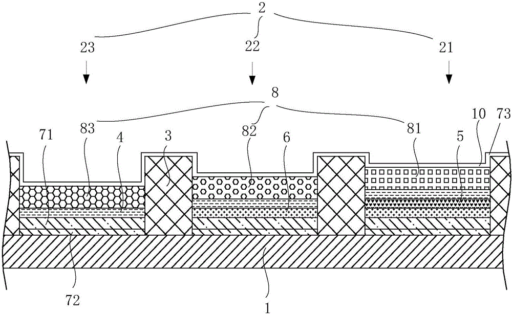
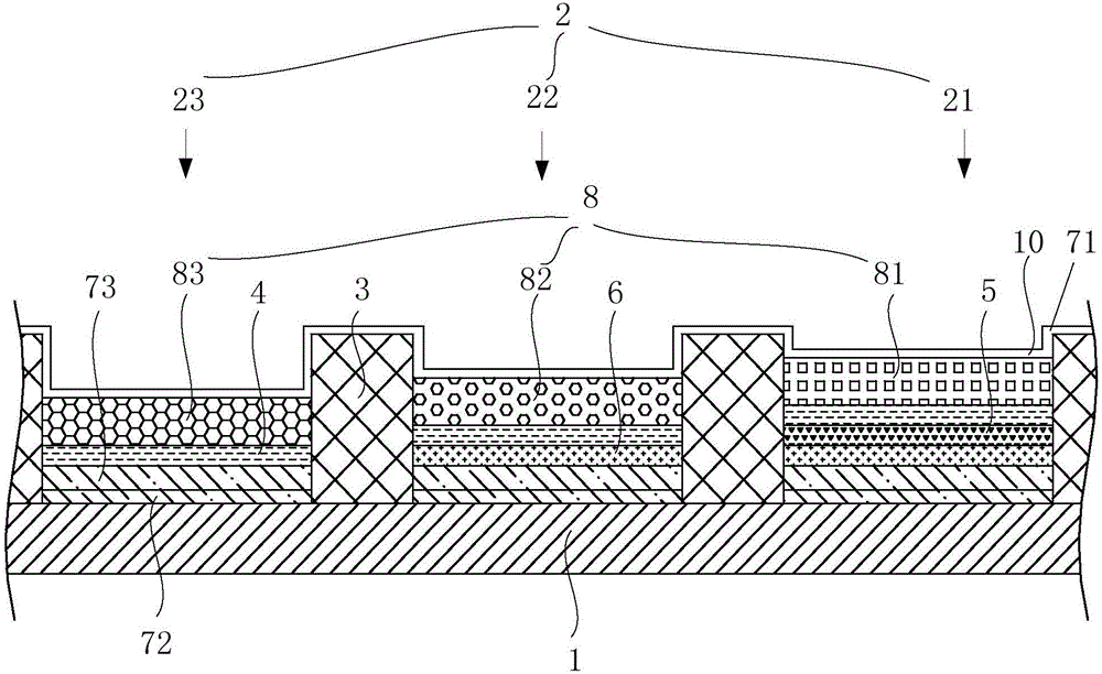
[0079] An embodiment of the present invention provides an organic light emitting diode array substrate, see figure 1 and figure 2 , the array substrate includes: a substrate 1, a plurality of sub-pixel units 2 disposed on the substrate 1;

[0080] Each sub-pixel unit 2 includes a compound electrode, an organic material functional layer 8 and a first electrode 10 sequentially arranged on the substrate 1; the thickness of the compound electrodes included in different types of sub-pixel units 2 is different;

[0081] The composite electrode, the organic material functional layer 8 and the first electrode 10 included in the same sub-pixel unit 2 form a microcavity structure.

[0082] In the organic light emitting diode array substrate in the embodiment of the present invention, a plurality of sub-pixel units 2 are arranged on the substrate 1, and the thicknesses of the composite electrodes included in different types of sub-pixel units 2 in the plurality of sub-pixel units 2 are...

Embodiment 2

[0123] An embodiment of the present invention provides a display device, which includes the organic light emitting diode array substrate described in Implementation 1.

[0124] The display device provided by this embodiment is easy to process and manufacture the organic light emitting diode array substrate, the manufacturing cost is low, and the manufacturing efficiency and yield are high, so that the display device has high yield and low cost.

Embodiment 3

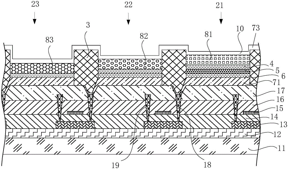
[0126] The present invention also provides a method for manufacturing an organic light emitting diode array substrate, see figure 1 and figure 2 , the production method includes:

[0127] forming a plurality of sub-pixel units 2 on the substrate 1;

[0128] Each sub-pixel unit 2 includes a composite electrode formed on the substrate 1, an organic material functional layer 8 formed on the composite electrode, and a first electrode 10 formed on the organic material functional layer 8; different types of sub-pixel units 2 include Composite electrodes have different thicknesses;

[0129] The composite electrode, the organic material functional layer 8 and the first electrode 10 included in the same sub-pixel unit 2 form a microcavity structure.

[0130] In the manufacturing method provided by the embodiment of the present invention, a plurality of sub-pixel units 2 are formed on the substrate 1, and the thicknesses of the composite electrodes included in different types of sub...


PUM


Abstract

The invention discloses an organic light-emitting diode array substrate, a display device and a manufacturing method, and belongs to the field of processing of displays. The array substrate comprises a substrate and a plurality of sub-pixel units, wherein the plurality of sub-pixel units are arranged on the substrate; each sub-pixel unit comprises a composite electrode, an organic material functional layer and a first electrode, which are sequentially arranged on the substrate; the composite electrodes included by different types of sub-pixel units are different in thickness; and the composite electrode, the organic material functional layer and the first electrode included by the same sub-pixel unit form a micro-cavity structure. The plurality of sub-pixel units are arranged on the substrate; and the composite electrodes included by different types of sub-pixel units in the plurality of sub-pixel units are different in thickness, so that the micro-cavity structures of different types of sub-pixel units are different in thickness; the manufacturing technology of the micro-cavity structures is simple and convenient to implement in process; the manufacturing cost is reduced; and the manufacturing efficiency and yield are improved.

Description

technical field [0001] The invention relates to the field of display processing, in particular to an organic light emitting diode array substrate, a display device and a manufacturing method. Background technique [0002] OLED (Organic Light-Emitting Diode, organic light-emitting diode) display device has ultra-light, ultra-thin, high brightness, large viewing angle, low voltage, low power consumption, fast response, high definition, shock resistance, bendable, low cost, simple process, With the advantages of less raw materials, high luminous efficiency and wide temperature range, it is considered to be the most promising new generation display technology. [0003] At present, due to the wide emission spectrum band of OLED light-emitting materials, the color purity of the required light source cannot be met, so the luminous efficiency and brightness of OLEDs are limited, resulting in low contrast and poor display effects of corresponding display devices. Using micro-resonat...

Claims


Application Information

Patent Timeline
Patent Type & Authority Applications(China)
IPC IPC(8): H01L27/32H01L51/52H01L51/56
CPCH10K59/35H10K50/805H10K71/00H10K59/122H10K50/816H10K50/818H10K50/852H10K2102/351H10K50/81H10K50/856H10K59/1201
Inventor 杨一帆
Owner BOE TECH GRP CO LTD
Why Eureka
Try Eureka