Fabrication method of floating gate

A floating gate, silicon wafer technology, applied in electrical components, circuits, semiconductor devices, etc., can solve the problems of increased maintenance frequency, poor particle state, etc., to improve flatness, remove particle problems, and increase the effect of cleaning processes

Inactive Publication Date: 2016-07-06
SHANGHAI HUALI MICROELECTRONICS CORP
View PDF3 Cites 3 Cited by
  • Summary
  • Abstract
  • Description
  • Claims
  • Application Information

AI Technical Summary

Problems solved by technology

Although the pits and particles of the original silicon wafer were eliminated by chemical mechanical polishing, the subsequent silicon wafers without grinding process brought particle problems, and the particle state of the machine was poor, which also increased the frequency of maintenance.

Method used


Image

  • Fabrication method of floating gate
  • Fabrication method of floating gate
  • Fabrication method of floating gate

Examples


Embodiment Construction

[0036] In order to make the content of the present invention clearer and easier to understand, the content of the present invention will be described in detail below in conjunction with specific embodiments and accompanying drawings.

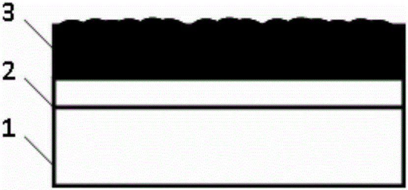
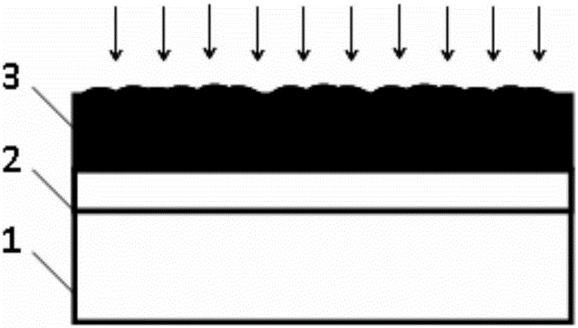
[0037] Figure 2 to Figure 6 Each step of the method for manufacturing a floating gate according to a preferred embodiment of the present invention is schematically shown.

[0038] Such as Figure 2 to Figure 6 As shown, the method for preparing a floating gate according to a preferred embodiment of the present invention includes:

[0039] The first step S1: perform the growth of the floating gate layer 3 on the tunnel oxide layer 2 (for example, the tunnel silicon dioxide layer) of the silicon wafer 1, such as figure 2 Shown:

[0040] Preferably, in the first step S1, the floating gate layer is prepared by a low pressure chemical vapor deposition (LPCVD) method in a furnace. For example, the reaction temperature is 620 degrees Celsius, and...


PUM


Abstract

The invention provides a fabrication method of a floating gate. The fabrication method comprises the following steps of 1, executing the growth of a floating gate layer on a tunnel oxide layer of a silicon wafer; 2, injecting into the floating gate layer; 3, executing rapid thermal annealing on the silicon wafer with O2 and N2 to form a thermal oxide layer on the surface of the floating gate layer; 4, removing the thermal oxide layer; and 5, grinding the floating gate layer. According to the method, a thermal annealing process is improved, a cleaning process of the oxide layer is additionally arranged, a chemical mechanical grinding process with high selection ratio is adopted, thus, particles during the annealing process are effectively removed, the flatness of poly-silicon of the floating gate is improved, and meanwhile, the maintenance frequency of an annealing machine is reduced.

Description

technical field [0001] The invention relates to the field of semiconductor manufacturing, and more specifically, the invention relates to a method for preparing a floating gate. Background technique [0002] As a non-volatile memory, flash memory (Flash) has the characteristics of non-volatility, high device density, low power consumption and electrical rewritability (electrical rewritability), and is widely used in portable electronic products such as mobile phones, digital cameras, smart cards Wait. [0003] The structure of a simple NOR flash memory floating gate transistor cell (Floating-gatetransistorCell) is as follows figure 1 As shown, the structure is roughly similar to a conventional MOS transistor. Specifically, a multilayer structure is arranged between the source electrode 20 and the drain electrode 30 on the surface of the substrate 10, and the multilayer structure includes a tunnel silicon dioxide layer 40, a floating gate 50, and a lower oxide layer 60 sequ...

Claims


Application Information

Patent Timeline
Patent Type & Authority Applications(China)
IPC IPC(8): H01L21/28
CPCH01L29/42324H01L29/401
Inventor 江润峰孙天拓
Owner SHANGHAI HUALI MICROELECTRONICS CORP
Why Eureka
Try Eureka