Supercharge Your Innovation With Domain-Expert AI Agents!

Stable nanowire field effect transistor taking gas as insulation layer and fabrication method of nanowire field effect transistor

A field effect transistor and insulating layer technology, which is applied in the field of nanowire field effect transistor and its preparation, can solve problems such as device failure and collapse of nanowire, and achieve the effect of structural stability

Inactive Publication Date: 2016-07-06
塔力哈尔·夏依木拉提
View PDF4 Cites 2 Cited by
  • Summary
  • Abstract
  • Description
  • Claims
  • Application Information

AI Technical Summary

Problems solved by technology

[0004] In view of the above problems, the object of the present invention is to provide a stable nanowire field effect transistor with gas as an insulating layer and its preparation method, which has a stable structure and avoids the collapse of the nanowire under the action of the induced electric field, and causes the device to fail to work. key issues of

Method used


Image

  • Stable nanowire field effect transistor taking gas as insulation layer and fabrication method of nanowire field effect transistor

Examples


Embodiment Construction

[0013] The present invention will be described in detail below in conjunction with the accompanying drawings and embodiments.

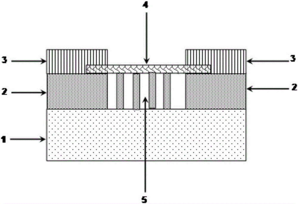
[0014] Such as figure 1 As shown, the present invention provides a stable gas-insulated nanowire field effect transistor, which includes a gate 1 , a support layer 2 , a source-drain electrode 3 , a micro-nano single crystal semiconductor 4 and a gas-gap insulating layer 5 . The gate 1 is a substrate, and a support layer 2 is provided on the top of the gate 1 , a source-drain electrode 3 is provided on both sides of the support layer 2 , and a micro-nano single crystal semiconductor 4 is provided between the two source-drain electrodes 3 . Below the micro-nano single-crystal semiconductor 4 between the two source-drain electrodes 3, a number of channels are longitudinally spaced apart on the supporting layer 2, and trenches are formed between adjacent channels; The grooves between the lower part of the semiconductor 4 and the support layer 2 form sev...


PUM


Abstract

The invention relates to a stable nanowire field effect transistor taking gas as an insulation layer and a fabrication method of the nanowire field effect transistor. The stable nanowire field effect transistor comprises a grid, a support layer, source-drain electrodes, a micro-nano single-crystal semiconductor and gas gap insulation layers, wherein the grid is a substrate, the support layer is arranged on the grid, one of the source-drain electrodes is arranged on each of the two sides of the upper part of the support layer, and the micro-nano single-crystal semiconductor is arranged between the two source-drain electrodes; the part, under the micro-nano single-crystal semiconductor between the two source-drain electrodes, of the support layer is provided with a plurality of channels in a longitudinal spaced manner, and grooves are formed between every two adjacent channels; and the upper part of the grid, the lower part of the micro-nano single-crystal semiconductor and the grooves at the middle of the support layer form the plurality of gas gap insulation layers. The field effect transistor is more stable in structure, a nanowire is prevented from being collapsed under the effect of an induced electric field, and the problem that the stable nanowire field effect transistor cannot normally work is prevented.

Description

technical field [0001] The invention relates to a field effect transistor and a preparation method, in particular to a stable nanowire field effect transistor with gas as an insulating layer and a preparation method. Background technique [0002] At present, the gate insulating layer plays a crucial role in the preparation of organic micro-nano single crystal field effect transistors. The gate insulators of organic micro-nano single-crystal transistors are mainly limited to silicon dioxide or OTS-modified silicon dioxide. The contact interface between the semiconductor and the insulating layer has a crucial impact on the performance of the sensor device. At the contact interface, phenomena such as carrier confinement, charge doping, molecular (or atomic) reorganization, dipole formation, and chemical interactions at the semiconductor / insulator interface are ubiquitous, thereby degrading the performance of the sensor device. [0003] In 2004, the research team of Rogers and...

Claims


Application Information

Patent Timeline
Patent Type & Authority Applications(China)
IPC IPC(8): H01L29/772H01L29/10H01L21/335B82Y10/00
CPCH01L29/772B82Y10/00H01L29/10H01L29/66409
Inventor 塔力哈尔·夏依木拉提李文亮彭敏冯艳谢宁
Owner 塔力哈尔·夏依木拉提
Features
  • R&D
  • Intellectual Property
  • Life Sciences
  • Materials
  • Tech Scout
  • Unparalleled Data Quality
  • Higher Quality Content
  • 60% Fewer Hallucinations
Learn More